Infrared focal plane detector

An infrared focal plane and detector technology, applied in the field of infrared detection, can solve the problems of low performance of infrared focal plane detectors, low pixel scale, poor consistency, etc., to reduce process difficulty and possible risks, small chip area, low cost effect

Active Publication Date: 2021-09-28
BEIJING NORTH GAOYE TECH CO LTD
View PDF8 Cites 3 Cited by
  • Summary
  • Abstract
  • Description
  • Claims
  • Application Information

AI Technical Summary

Problems solved by technology

[0010] In order to solve the above-mentioned technical problems or at least partly solve the above-mentioned technical problems, the present disclosure provides an infrared focal plane detector, which solves the problems of low performance, low pixel scale, low yield and poor consistency of traditional MEMS process infrared focal plane detectors. It is beneficial to improve the structural stability of the infrared focal plane detector, increase the area of ​​the absorbing plate, improve the infrared detection sensitivity of the infrared focal plane detector, and improve the absorption rate of the infrared focal plane detector to the incident infrared electromagnetic wave. Optimize the performance of infrared focal plane detectors and reduce the difficulty of optical design of infrared focal plane detectors

Method used


Image

  • Infrared focal plane detector
  • Infrared focal plane detector
  • Infrared focal plane detector

Examples


Embodiment Construction

[0065] In order to more clearly understand the above objects, features and advantages of the present disclosure, the solutions of the present disclosure will be further described below. It should be noted that, in the case of no conflict, the embodiments of the present disclosure and the features in the embodiments can be combined with each other.

[0066] In the following description, many specific details are set forth in order to fully understand the present disclosure, but the present disclosure can also be implemented in other ways than described here; obviously, the embodiments in the description are only some of the embodiments of the present disclosure, and Not all examples.

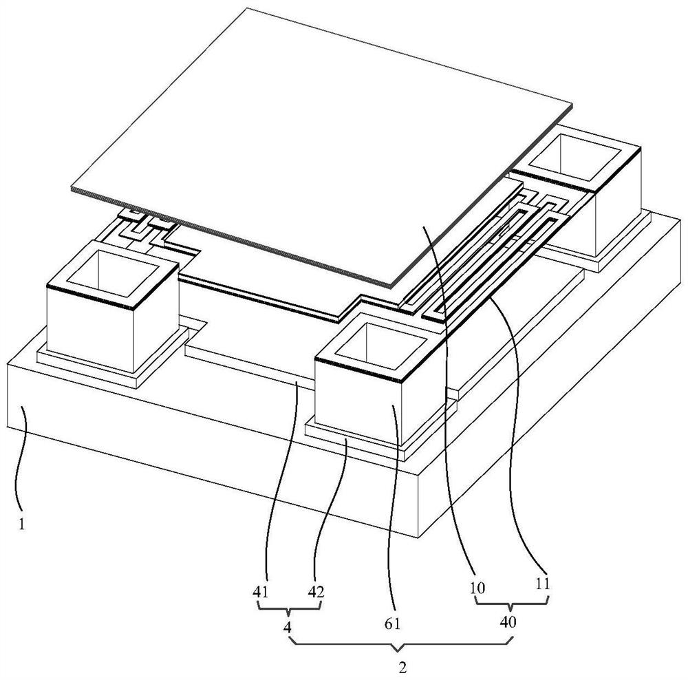
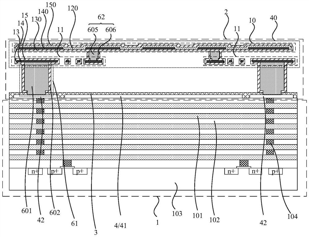
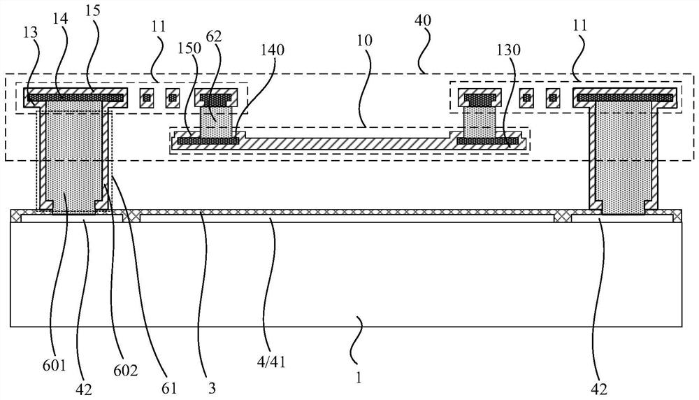
[0067] figure 1 A schematic diagram of a three-dimensional structure of an infrared focal plane detector pixel provided by an embodiment of the present disclosure, figure 2 A schematic cross-sectional structure diagram of an infrared focal plane detector pixel provided by an embodiment of the ...


PUM


Abstract

The invention relates to an infrared focal plane detector, a CMOS measurement circuit system and a CMOS infrared sensing structure in the infrared focal plane detector are both prepared by using a CMOS process, in the infrared focal plane detector, a first columnar structure is located between a reflecting layer and a beam structure, a second columnar structure is located between an absorption plate and the beam structure, the first columnar structure and the second columnar structure are solid columnar structures, and the infrared focal plane detector further comprises a metamaterial structure and / or a polarization structure. Through the technical scheme of the invention, the problems of low performance, low pixel scale, low yield and poor consistency of a traditional MEMS process infrared focal plane detector are solved, the structural stability of the infrared focal plane detector is improved, the area of the absorption plate is increased, the infrared detection sensitivity of the infrared focal plane detector is improved, the absorption rate of the infrared focal plane detector to incident infrared electromagnetic waves is improved, the performance of the infrared focal plane detector is optimized, and the difficulty of optical design of the infrared focal plane detector is reduced.

Description

technical field [0001] The present disclosure relates to the technical field of infrared detection, in particular to an infrared focal plane detector. Background technique [0002] Surveillance market, automotive auxiliary market, home furnishing market, intelligent manufacturing market, and mobile phone applications all have strong demand for uncooled high-performance chips, and have certain requirements for chip performance, performance consistency, and product prices. It is estimated that there is a potential demand of more than 100 million chips every year, but the current process scheme and architecture cannot meet the market demand. [0003] At present, the infrared focal plane detector adopts the method of combining the measurement circuit and the infrared sensing structure. -Electro-Mechanical System, micro-electro-mechanical system) process preparation, resulting in the following problems: [0004] (1) The infrared sensing structure is prepared by MEMS technology,...

Claims


Application Information

Patent Timeline
Patent Type & Authority Applications(China)
IPC IPC(8): G01J5/24
CPCG01J5/24Y02P70/50
Inventor 翟光杰潘辉武佩翟光强
Owner BEIJING NORTH GAOYE TECH CO LTD
Why Eureka
Try Eureka