
Chip weakening structure, manufacturing method thereof, mass transfer method and display panel

A chip and vertical structure technology, applied in electrical components, electric solid state devices, circuits, etc., can solve the problem of low transfer efficiency of Micro-LED chips in large quantities, and achieve the effect of improving transfer accuracy

Active Publication Date: 2021-09-28
SHENZHEN SITAN TECH CO LTD
View PDF4 Cites 2 Cited by
  • Summary
  • Abstract
  • Description
  • Claims
  • Application Information

AI Technical Summary

Problems solved by technology

Especially the problem of low mass transfer efficiency of vertical Micro-LED chips

Method used


Image

  • Chip weakening structure, manufacturing method thereof, mass transfer method and display panel
  • Chip weakening structure, manufacturing method thereof, mass transfer method and display panel
  • Chip weakening structure, manufacturing method thereof, mass transfer method and display panel

Examples


Embodiment Construction

[0080] As mentioned in the background technology section, mass transfer is the core technical problem faced in the process of Micro-LED industrialization at present. Micro-LED chips must first be bonded to substrates made of silicon or sapphire during the manufacturing process, and then peeled off by laser. The silicon or sapphire substrate is removed, and then the Micro-LED chip is transferred onto the driving circuit substrate. In the process of mass transfer, after the silicon or sapphire substrate is removed by laser lift-off, the Micro-LED chip will fall off from the substrate, and multiple independent single LED chips will be formed, which are randomly arranged and their positions are not fixed, resulting in During the mass transfer process, it is difficult to position a single Micro-LED chip when clamping or adsorbing, and when transferring to the drive circuit substrate, the position of the Micro-LED chip is difficult to control, resulting in a cumbersome and time-consu...


PUM


Abstract

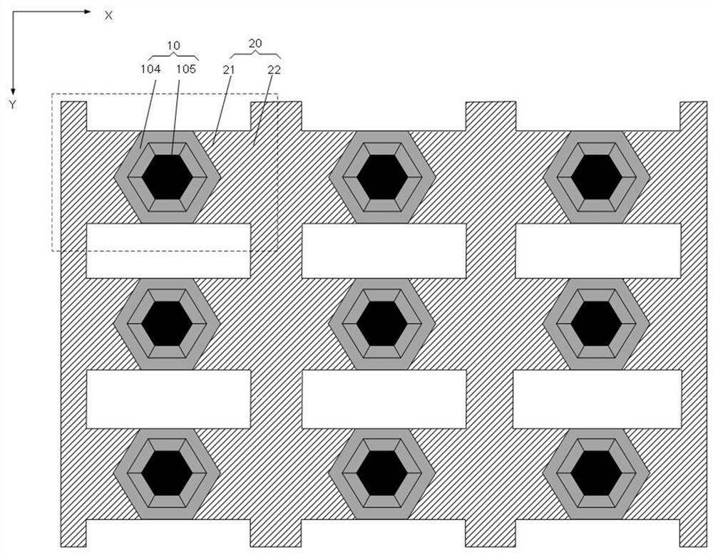
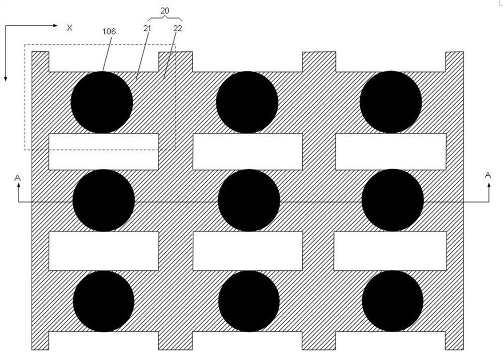
The invention discloses a chip weakening structure, a manufacturing method of the chip weakening structure, a mass transfer method and a display panel. The LED chip weakening structure comprises a plurality of Micro-LED chips and connecting bridges located between the adjacent Micro-LED chips. On the one hand, the connecting bridge plays a role in temporary connection, and the problems of poor precision and low efficiency of mass transfer caused by random scattering of the Micro-LED chips with the vertical structures after falling off from the substrate are avoided; on the other hand, the connecting bridges fix the positions of the Micro-LED chips of the vertical structures, so the Micro-LED chips of the vertical structures can be conveniently positioned by a clamping or adsorption device in the mass transfer process, the transfer precision can be improved, and mass transfer can be quickly realized.

Description

technical field [0001] The present invention relates to the field of semiconductor manufacturing technology, and in particular to a weakened structure of a Micro-LED chip and a manufacturing method thereof, a mass transfer method of a Micro-LED chip, and a micro-LED chip formed based on a weakened structure of a Micro-LED chip and a mass transfer method. Micro-LED display panel. Background technique [0002] Micro Light Emitting Diode (Micro Light Emitting Diode, Micro-LED) has the characteristics of self-luminous display. It is an all-solid-state light-emitting diode with long life, high brightness, low power consumption, small size, and ultra-high resolution. It can be applied in extreme environments such as high temperature or radiation. Compared with OLED technology, which is also a self-luminous display, Micro-LED not only has higher efficiency, longer life, relatively stable materials, is not easily affected by the environment, and can also avoid image sticking. [0...

Claims


Application Information

Patent Timeline
Patent Type & Authority Applications(China)
IPC IPC(8): H01L27/15H01L33/00
CPCH01L27/156H01L33/0093H01L33/0095
Inventor 刘召军杨杭张珂
Owner SHENZHEN SITAN TECH CO LTD
Learn More