

A single event effect pulsed laser test method for gan power devices
A single event effect and power device technology, which is applied in electronic circuit testing, non-contact circuit testing, etc., can solve the problems of test method and model accuracy drop, improve experimental efficiency and accuracy, make up for machine time constraints, The effect of reducing the cost of experiments
Active Publication Date: 2022-02-22
NAT SPACE SCI CENT CAS
View PDF9 Cites 0 Cited by
- Summary
- Abstract
- Description
- Claims
- Application Information
AI Technical Summary
Problems solved by technology
Due to the limitations of the special physical absorption mechanism of the wide-bandgap semiconductor device laser and different optical modulation methods, the accuracy of the test method and model has declined.
Method used
View moreImage
Smart ImageViewing Examples

Examples
Embodiment
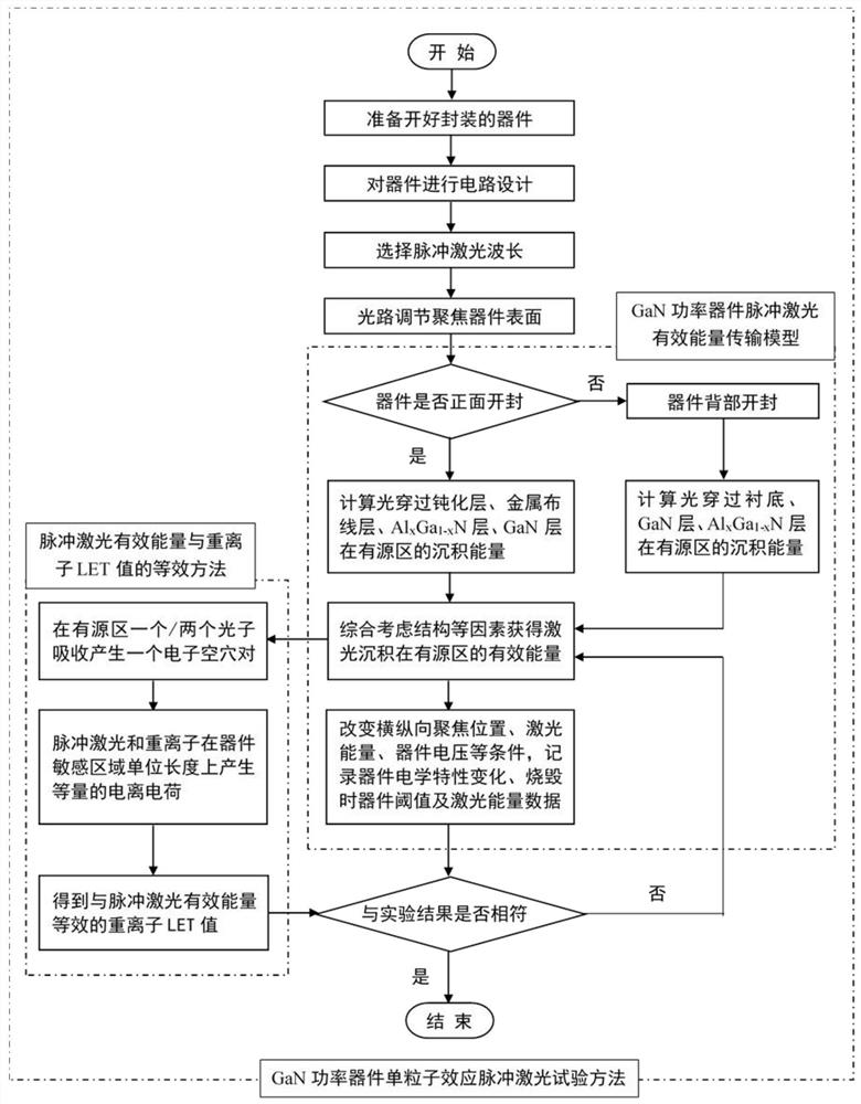
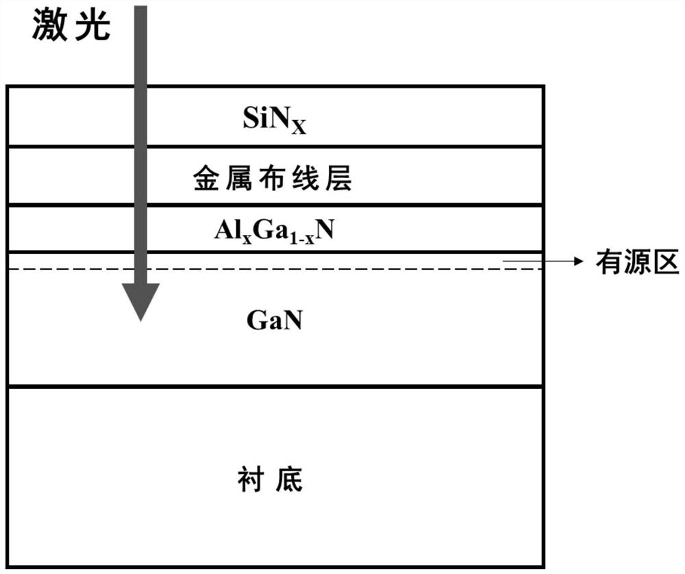
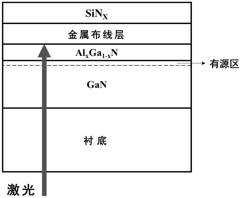
[0041] Refer figure 1 As shown, the present invention provides a single-particle effect pulse laser test method of GaN power devices, which includes the following steps:
[0042] S1, the encapsulating GaN power device is opened from the front or back to obtain a GaN power device, ie the GaN power device;
Login to View More PUM
 Abstract
The invention discloses a GaN power device single-event effect pulsed laser test method, which utilizes the GaN power device single-event effect single- and two-photon absorption mechanism pulse laser equivalent heavy ion evaluation technology, and innovatively adopts a technical method combining theory and experiment ;Taking GaN power devices as a typical application demonstration, aiming at the experimental requirements of single event effects of wide bandgap devices, a theoretical model of the effective energy and equivalent LET value of GaN samples deposited by pulsed laser front and back radiation is formed, and the characterization of the laser quantitative evaluation test is clarified Method and basis: To carry out the comparison test of laser and heavy ion on the sensitivity of single event effect, and to determine the corresponding relationship between the laser effective energy of the device and the LET value of heavy ion. The method of the invention can be used as an important supplement for heavy ion experiments, reduce the cost of experiments, improve the efficiency and accuracy of experiments, and provide test references for the selection of anti-radiation devices and the design of anti-radiation reinforcement in practical applications.
Description
Technical field [0001] The present invention belongs to the evaluation of aerospace electronics radiation effects and reinforcement design, in particular to a single-particle effect pulse laser test method for GaN power devices. Background technique [0002] The gallium nitride (GaN) is used as a third-generation semiconductor material, which is considered to be a semiconductor material that is the most developed since the first generation of semiconductor material silicon (Si), the second-generation semiconductor material arsenide (GaAs) or the like. Although the SI base device is close to the theoretical limit, there is still a certain gap with the third generation of semiconductor performance, and the development space of GaN material is larger. GaN is banned, high-tee, high electron saturation drift speed, high melting point, low pond-state resistance, high breakdown voltage, high anti-radiation performance, these characteristics determine GaN to manufacture high temperature,...
Claims
Login to View More Application Information
Patent Timeline
 Patent Type & Authority Patents(China)
IPC IPC(8): G01R31/311
CPCG01R31/311
Inventor 马英起崔艺馨韩建伟上官士鹏王英豪
Owner NAT SPACE SCI CENT CAS