A high-stability packaging structure for semiconductors

A technology with high stability and packaging structure, which is applied in the direction of semiconductor devices, semiconductor/solid-state device components, electric solid-state devices, etc., and can solve problems such as connection offset, unreliable electrical connection, and reduced stability of electrical connection. Achieve the effect of overcoming gaps and offset problems, not easy to be disturbed or polluted by the outside world, and low process difficulty

Active Publication Date: 2021-11-05
HAIMEN JINQILIN REDWOOD INVESTMENT DEV
View PDF5 Cites 0 Cited by
  • Summary
  • Abstract
  • Description
  • Claims
  • Application Information

AI Technical Summary

Problems solved by technology

[0004] However, when the metal bumps on the chip are connected to the conductive medium in the through hole, on the one hand, there are likely to be gaps and the electrical connection is unreliable. The phenomenon of shifting will significantly reduce the stability of electrical connections, thereby reducing the packaging quality of semiconductors, especially for more expensive and important semiconductor devices, the impact of unstable conductive connections is greater

Method used


Image

  • A high-stability packaging structure for semiconductors
  • A high-stability packaging structure for semiconductors
  • A high-stability packaging structure for semiconductors

Examples


Embodiment 1

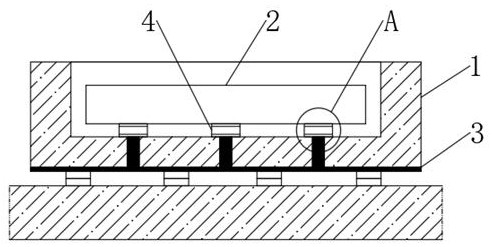
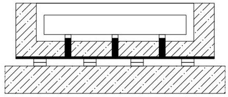
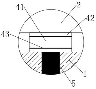
[0044] see Figure 1-3 , a high-stability packaging structure for semiconductors, including an adapter board 1 and a PCB board, the upper end of the adapter board 1 is provided with a receiving groove, the receiving groove is embedded with a chip 2, and the lower end of the chip 2 is provided with a plurality of evenly distributed metal Bumps, the lower end of the adapter board 1 is provided with a redistribution circuit 3, and the redistribution circuit 3 is welded to the PCB board through multi-point welding. A plurality of conductive holes matching the metal bumps are opened on the bottom wall of the storage tank. It is filled with a conductive medium 5, and a positioning conductive disk 4 is installed between the conductive medium 5 and the corresponding metal bump. The positioning conductive disk 4 includes a hollow base disk 41, a pair of thermosetting adhesive disks 42 and a pair of bonding middle films 43, The bonding film 43 is symmetrically attached to the upper and ...


PUM


Abstract

The invention discloses a high-stability packaging structure for semiconductors, which belongs to the technical field of semiconductors. The invention can conduct conductive connection to the metal bumps on the chip and the conductive medium in the conductive hole by introducing a positioning conductive plate. Compared with the traditional Contact electrical connection, the positioning of the conductive plate can not only rely on the thermosetting adhesive plate for effective positioning, and it is not easy to be deviated, but also use the deformable characteristics of the bonding film to provide the reliability of the interface connection, which can effectively overcome the difficulties in traditional packaging technology. There are gaps and offset problems, and it can be isolated and protected to a certain extent, and it is not easy to be disturbed or polluted by the outside world, thereby greatly improving the stability of the conductive connection, and the process is relatively difficult, suitable for large-scale promotion.

Description

technical field [0001] The invention relates to the technical field of semiconductors, and more specifically relates to a high-stability packaging structure for semiconductors. Background technique [0002] Semiconductor packaging refers to the process of processing the tested wafers according to the product model and functional requirements to obtain independent chips. The packaging process is: the wafer from the wafer front-end process is cut into small chips after the dicing process, and then the cut chips are glued to the small island of the corresponding substrate (lead frame) frame, and then Use ultra-fine metal (gold-tin-copper-aluminum) wires or conductive resin to connect the bonding pads of the chip to the corresponding pins of the substrate to form the required circuit; then the independent chip is packaged and protected with a plastic case. After plastic sealing, a series of operations are required. After the packaging is completed, the finished product is teste...

Claims


Application Information

Patent Timeline
Patent Type & Authority Patents(China)
IPC IPC(8): H01L23/498H01L23/31
CPCH01L23/49838H01L23/49811H01L23/3107
Inventor 吴祖恒陈丹红
Owner HAIMEN JINQILIN REDWOOD INVESTMENT DEV
Why Eureka
Try Eureka