
High-density static random access memory bit unit structure and process method thereof

A bit cell, static random technology, applied in semiconductor/solid-state device manufacturing, electrical components, semiconductor devices, etc., can solve the problems of unreasonable bit cell structure, high power consumption and cost, and poor high-density characteristics of static random access memory. Achieve the effect of reducing active area area, reducing power consumption and cost, and improving high-density characteristics

Pending Publication Date: 2021-10-08
GUANGDONG GREATER BAY AREA INST OF INTEGRATED CIRCUIT & SYST +1
View PDF0 Cites 0 Cited by
  • Summary
  • Abstract
  • Description
  • Claims
  • Application Information

AI Technical Summary

Problems solved by technology

[0004] Aiming at the problems of unreasonable structure of SRAM bit cells in the prior art, resulting in poor high-density characteristics, high power consumption and high cost, the present invention provides a high-density SRAM bit cell structure and its process method , its structural design is simple and reasonable, which can improve the high-density characteristics of the bit cell, and at the same time reduce power consumption and cost

Method used


Image

  • High-density static random access memory bit unit structure and process method thereof
  • High-density static random access memory bit unit structure and process method thereof
  • High-density static random access memory bit unit structure and process method thereof

Examples


Embodiment Construction

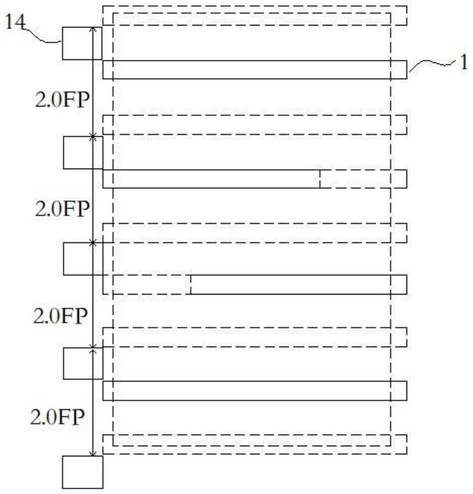
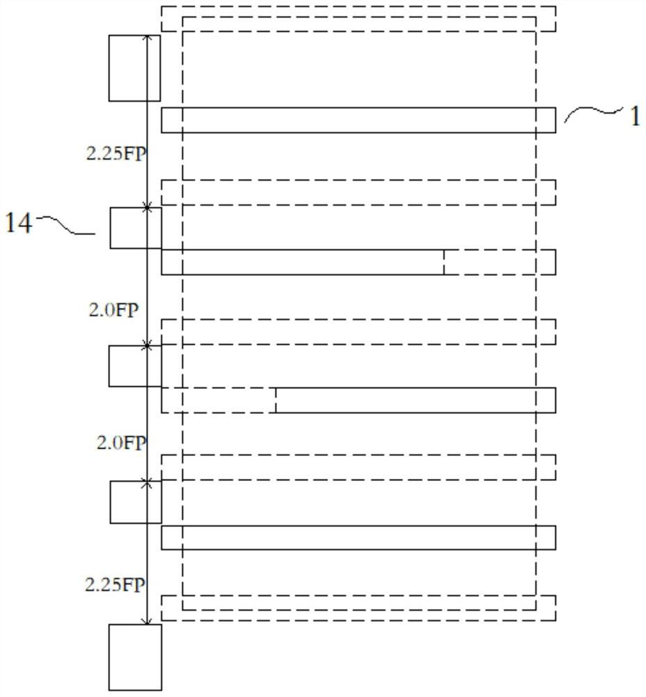
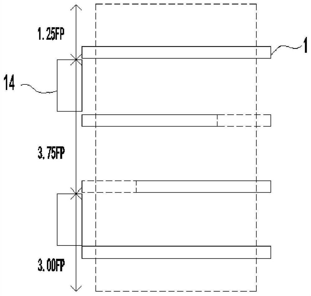
[0033] See image 3 and Figure 4 , a high-density SRAM bit cell structure, which includes a substrate, fins 1 distributed on the surface of the substrate, gate regions 2 distributed on the fins 1, a photoresist layer 14, a contact layer 4, a read The bit line 5, the substrate is silicon, the bit unit includes a 22nm fin field effect transistor 6, the fin field effect transistor 6 is a PMOS transistor, including two fins, a gate region, a contact layer, and a part for reading the bit line Area; fin 1 includes four: the first fin, the second fin, the third fin, and the fourth fin, and are distributed in parallel at intervals in sequence, wherein the tail of the second fin and the head of the third fin are cutting areas. Assuming that the fin pitch between two adjacent fins 1 is FP, and the contact layer pitch is CPP, then the total vertical width of the active area of ​​the bit cell is 8*FP, and the total vertical width of the active area is the total fin pitch direction. Th...


PUM


Abstract

The invention discloses a high-density static random access memory bit unit structure and a process method thereof, which can improve the high-density performance of a bit unit and reduce power consumption and cost. The high-density static random access memory bit unit structure comprises a substrate, fins distributed on the surface of the substrate, gate regions distributed on the fins, a photoresist layer, a contact layer and a read bit line, wherein the bit unit comprises a fin-shaped field effect transistor, the length of each gate region is 22 nm, four fins are sequentially distributed at intervals in parallel, the fin distance between every two adjacent fins is FP, the contact layer distance is CPP, the vertical total width of an active region of the bit unit is 8*FP, the transverse total width of the active region is 2*CPP, and the minimum area of the active region of the bit unit is 0.0739 mu m<2>. The process method comprises the steps that: a self-alignment double pattern transfer process is adopted, the bit unit which comprises the four fins is obtained, the fin distance between every two adjacent fins is FP, the bit unit needs two photoresist layers, and the four fins are obtained through a photoetching process.

Description

technical field [0001] The invention relates to the technical field of field effect transistors, in particular to a high-density static random access memory bit unit structure and a process method thereof. Background technique [0002] Static random access memory (SRAM) is a memory device used for random access to data. "Static" means that the memory can keep the stored data constant when it is powered on. Static random access memory contains bit units, which are usually used as caches for CPU / GPU calculations. At present, SRAM bit units in highly integrated circuit chips account for about 30% to 60% of the entire chip area, of which The 6T high-density static random access memory (6T HD SRAM) containing six transistors is used more frequently. The main technical indicators of 6T HD SRAM include power consumption, unit area (for identifying density characteristics), process, and unit cost. Through the above indicators, each process technology node of 6T HD SRAM can be measu...

Claims


Application Information

Patent Timeline
Patent Type & Authority Applications(China)
IPC IPC(8): H01L27/11H01L21/8244H01L29/78H01L29/10H10B10/00
CPCH01L29/785H01L29/1033H10B99/00H10B10/12
Inventor 黄国泰苏炳熏叶甜春罗军赵杰
Owner GUANGDONG GREATER BAY AREA INST OF INTEGRATED CIRCUIT & SYST
Learn More