Optically-transparent semiconductor buffer layers and structures employing the same
An optically transparent and buffer layer technology, applied in semiconductor devices, photovoltaic power generation, electrical components, etc., can solve the problems of increasing optical absorption and increasing the value of lattice constant
- Summary
- Abstract
- Description
- Claims
- Application Information
AI Technical Summary
Problems solved by technology
Method used
Image
Examples
example 1
[0060] Example 1 (using AlP x Sb 1-x )
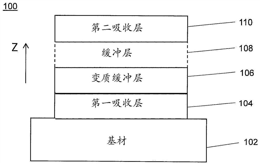
[0061] described in Table 1 around the AlP x Sb 1-x and configured to provide a non-limiting example of a specific metamorphic buffer layer structure that transitions between the lattice constants of GaAs and GaSb. In this and other examples, the value of "absorption edge" refers to and defines the wavelength corresponding to the spectral cutoff of absorption of a semiconductor material in which light of wavelengths shorter than the cutoff wavelength is absorbed.
[0062] Table 1 Examples of metamorphic buffer layers
[0063]
[0064]
[0065] In one case, with AlP 0.71 Sb 0.29 Composed materials are approximately lattice-matched to GaAs and have AlP 0.06 Sb 0.94 The composed material is approximately lattice-matched to GaSb. The minimum bandgaps of the metamorphic buffer layers of Table 1 vary between approximately 1.27 eV and 1.64 eV, corresponding to long wavelength absorption edges between 755 nm and 960 nm. In su...
example 2
[0068] Example 2 (using GaP x Sb 1-x ):
[0069] Table 2 shows the surrounding GaP x Sb 1-x A non-limiting example of a specific metamorphic buffer layer constructed and configured to provide a transition between the lattice constants of GaAs and GaSb.
[0070] Table 2: Examples of metamorphic buffer layers (using GaPSb)
[0071]
[0072] In one case, with GalP 0.68 Sb 0.29 The composition of the material is approximately lattice-matched to GaAs, and has GaSb 0The composition of the material is lattice matched to GaSb. The minimum bandgap of the metamorphic buffer layers of Table 2 varies between about 0.67 eV and 1.22 eV, which corresponds to a long wavelength absorption edge between 1020 nm and 1860 nm. Light having wavelengths in excess of about 1860 nm should not experience any appreciable absorption when passing through or propagating in such a metamorphic buffer layer. Therefore, this layer is practically and operationally suitable to facilitate the applic...
example 3
[0073] Example 3 (using AlAs x Sb 1-x )
[0074] Table 3 gives the surrounding AlAs x Sb 1-x and configured to provide a non-limiting example of a specific metamorphic buffer layer structure that provides a transition between the lattice constants of GaSb and GaAs.
[0075] Table 3: Examples of metamorphic buffer layers (using AlAsSb)
[0076]
[0077]
[0078] In one instance, a material with an AlSb composition is approximately lattice matched to GaSb, and a material with an AlAs composition is approximately lattice matched to GaAs. The minimum bandgaps of the metamorphic buffer layers of Table 3 vary between approximately 1.58 eV and 2.15 eV, corresponding to long wavelength absorption edges between 785 nm and 577 nm. In such a metamorphic buffer layer, light having a wavelength in excess of about 785 nm should not experience any appreciable absorption while propagating through or in such a metamorphic buffer layer. Therefore, this layer is practically and op...
PUM
| Property | Measurement | Unit |
|---|---|---|
| thickness | aaaaa | aaaaa |
| thickness | aaaaa | aaaaa |
| thickness | aaaaa | aaaaa |
Abstract
Description
Claims
Application Information
 - R&D
- Intellectual Property
- Life Sciences
- Materials
- Tech Scout
- Unparalleled Data Quality
- Higher Quality Content
- 60% Fewer Hallucinations
Browse by: Latest US Patents, China's latest patents, Technical Efficacy Thesaurus, Application Domain, Technology Topic, Popular Technical Reports.
© 2025 PatSnap. All rights reserved.Legal|Privacy policy|Modern Slavery Act Transparency Statement|Sitemap|About US| Contact US: help@patsnap.com


