A chip stack and its preparation method

A chip stacking and carrier technology, which is applied in semiconductor/solid-state device manufacturing, semiconductor devices, electric solid-state devices, etc., can solve the problems of polluting the active area of ​​semiconductor components and poor bonding stability of semiconductor components

Active Publication Date: 2021-11-12
NANTONG HUIFENG ELECTRONICS TECH
View PDF6 Cites 0 Cited by
  • Summary
  • Abstract
  • Description
  • Claims
  • Application Information

AI Technical Summary

Problems solved by technology

In the chip stacking process, when an organic adhesive material is placed on a semiconductor element, and another semiconductor element is placed on the semiconductor element, due to the fluidity of the organic adhesive material, the organic adhesive material will flow from the two Overflow in the gap of the semiconductor element, on the one hand leads to contamination of the active area of ​​the semiconductor element by the organic adhesive material, and on the other hand leads to poor bonding stability of the two semiconductor elements

Method used


Image

  • A chip stack and its preparation method
  • A chip stack and its preparation method
  • A chip stack and its preparation method

Examples


Embodiment Construction

[0036] In order to better understand the technical solutions of the present invention, the embodiments of the present invention will be described in detail below in conjunction with the accompanying drawings. Based on the embodiments of the present invention, all other embodiments obtained by persons of ordinary skill in the art without creative efforts fall within the protection scope of the present invention.

[0037] The present invention proposes a method for preparing a chip stack, comprising the following steps:

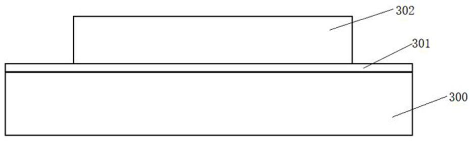
[0038] Step (1): A first carrier is provided, a first adhesive layer is arranged on the first carrier, a plurality of first semiconductor elements are arranged on the first adhesive layer, and the functional areas of the first semiconductor elements contacting the first adhesive layer.

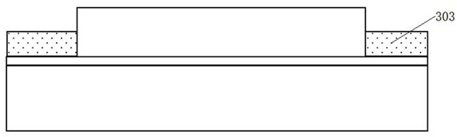
[0039] Step (2): disposing a first sacrificial material layer on the first bonding layer, the first sacrificial material layer wrapping the side of the first semiconductor ele...


PUM


Abstract

The present invention relates to a chip stack and a preparation method thereof. By forming a first annular protrusion and a second annular protrusion on the top surface of the first semiconductor element, the first annular protrusion surrounds the second annular protrusion, the first annular protrusion includes a plurality of a first sub-bump region, a plurality of second sub-bump regions and a plurality of third sub-bump regions, and the top surface of the second semiconductor element is etched to A first annular groove, a second annular groove, and a plurality of third grooves connecting the first annular groove and the second annular groove are formed on the top surface of the first annular groove, and the first annular groove surrounds the A second annular groove, followed by embedding a first annular protrusion into the first annular groove by using an adhesive material, and embedding the second annular protrusion into the second annular groove.

Description

technical field [0001] The invention relates to the field of semiconductor packaging, in particular to a chip stack and a preparation method thereof. Background technique [0002] In an existing chip stack, a plurality of semiconductor elements are vertically stacked together through an organic adhesive material, and after the stacking process is completed, the chip stack is then wrapped by a molding process. In the chip stacking process, when an organic adhesive material is placed on a semiconductor element, and another semiconductor element is placed on the semiconductor element, due to the fluidity of the organic adhesive material, the organic adhesive material will flow from the two The overflow in the gap of the semiconductor element will, on the one hand, cause the organic adhesive material to contaminate the active area of ​​the semiconductor element, and on the other hand, lead to poor bonding stability of the two semiconductor elements. Contents of the invention ...

Claims


Application Information

Patent Timeline
Patent Type & Authority Patents(China)
IPC IPC(8): H01L21/50H01L21/56H01L23/31
CPCH01L21/50H01L21/561H01L21/568H01L23/3185H01L23/3178H01L23/3171
Inventor 宋小波石明华蔡成俊陈健
Owner NANTONG HUIFENG ELECTRONICS TECH
Why Eureka
Try Eureka