Liquid crystal display panel and display device
A liquid crystal display panel and non-display area technology, applied in the direction of instruments, nonlinear optics, optics, etc., can solve the problems of electrode damage, weak antistatic ability of the display panel, etc., and achieve the effect of enhancing antistatic ability
- Summary
- Abstract
- Description
- Claims
- Application Information
AI Technical Summary
Problems solved by technology
Method used
Image
Examples
Embodiment 1
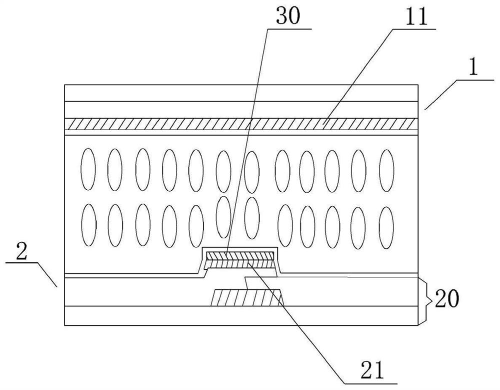
[0046] refer to figure 1 , the liquid crystal display panel provided in Embodiment 1 of the present application includes a color filter substrate 1 and an array substrate 2;
[0047] Wherein, the color filter substrate 1 includes a first electrode layer 11; the array substrate 2 includes a base substrate 20 and a second electrode layer 21 disposed on the base substrate 20; the second electrode layer 21 is provided with an insulating layer 30 and / or An insulating layer 30 is disposed on the first electrode layer 11 , and the orthographic projection of the insulating layer 30 on the base substrate 20 at least partially overlaps with the orthographic projection of the second electrode layer 21 on the base substrate 20 .
[0048]According to the liquid crystal display panel provided by the embodiment of the present application, the insulating layer 30 is provided on the first electrode layer 11 and / or the second electrode layer 21, and the orthographic projection of the insulating...
Embodiment 2
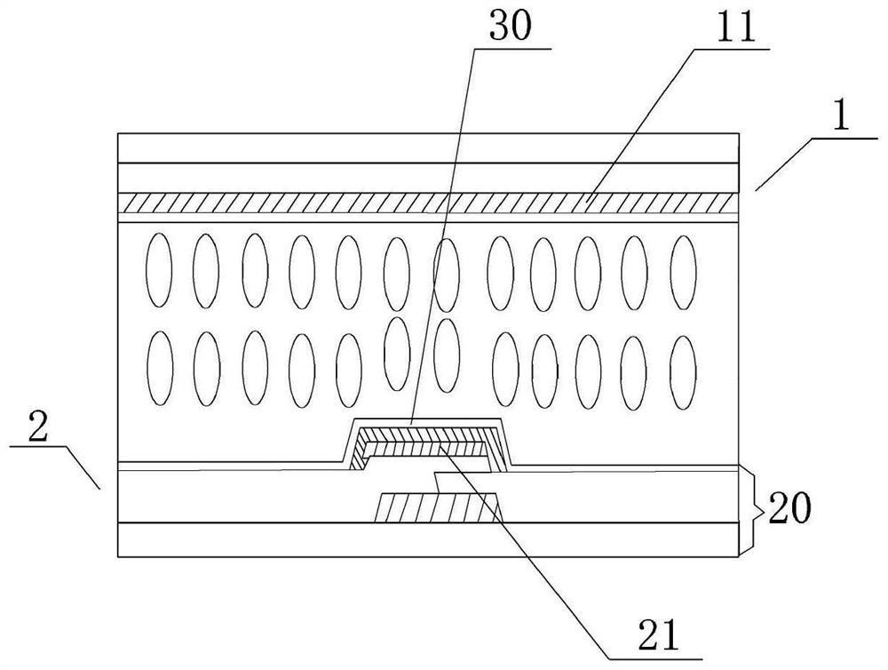
[0062] refer to figure 2 , in the second embodiment of the present application, the insulating layer 30 wraps the second electrode layer 21, that is, the surface of the second electrode layer 21 facing the first electrode layer 11 and the side surface of the second electrode layer 21 are covered with the insulating layer 30, so that Not only is there an insulating layer 30 between any position of the surface of the second electrode layer 21 facing the first electrode layer 11 and the first electrode layer 11, but there is also an insulating layer 30 between the side of the second electrode layer 21 and the first electrode layer 11. The insulation layer 30 can prevent the first electrode layer 11 from passing through the side of the second electrode layer 21 and the arc discharge between the second electrode layer 21. In this case, even if the first electrode layer 11 and the second electrode layer If the distance between the electrode layers 21 is too small, arc discharge wil...
Embodiment 3
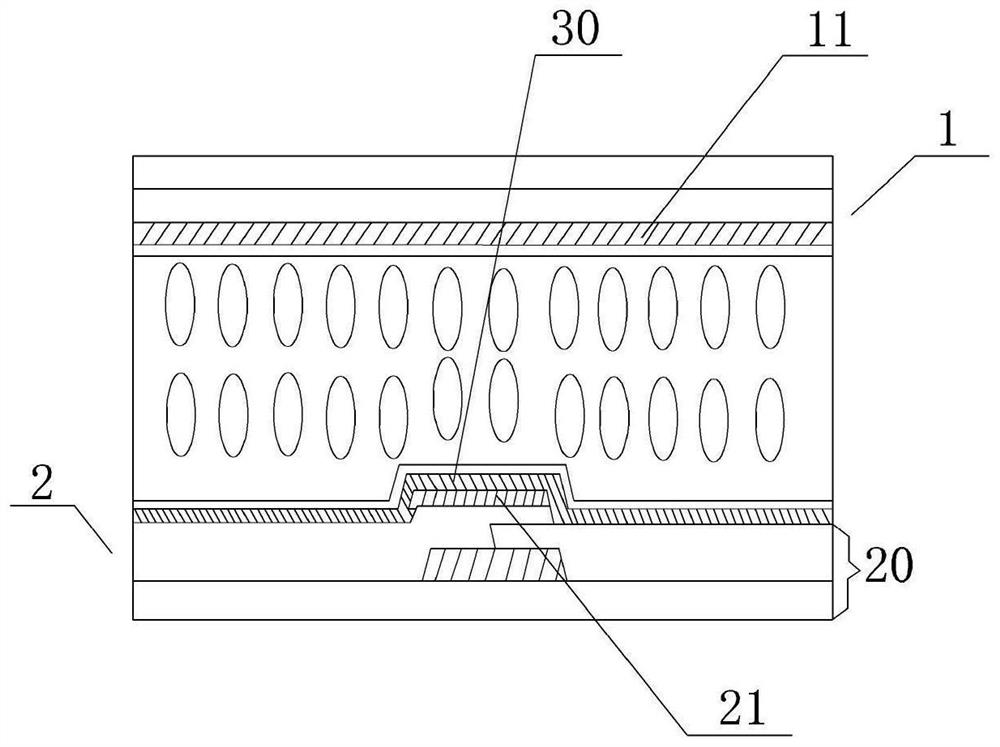
[0065] refer to image 3 , in the third embodiment of the present application, the insulating layer 30 covers the base substrate 20 and wraps the second electrode layer 21 . In order to make the insulating layer 30 have a better barrier effect between the first electrode layer 11 and the second electrode layer 21, the insulating layer 30 can also cover the base substrate 20 and wrap the second electrode layer 21, so that a relatively large The large-area insulating layer 30 completely covers the base substrate 20 and the second electrode layer 21, which makes it more convenient for the insulating layer 30 to be quickly disposed on the second electrode layer 21, and the surface of the second electrode layer 21 even the base substrate 20 The surface of each is fully covered with the insulating layer 30, which can ensure that arc discharge does not occur between the first electrode layer 11 and the second electrode layer 21, and enhances the antistatic ability of the liquid cryst...
PUM
| Property | Measurement | Unit |
|---|---|---|
| thickness | aaaaa | aaaaa |
| electrical resistivity | aaaaa | aaaaa |
Abstract
Description
Claims
Application Information


