Active circuit printed board, phased-array antenna and manufacturing process thereof

A technology of phased array antennas and active circuits, which is applied to the manufacture of antenna array devices, antennas, circuits, etc., can solve the problems of low efficiency, high processing cost, and difficult processing, so as to reduce difficulty, improve processing efficiency, Effect of reducing wiring complexity

Pending Publication Date: 2021-10-22
CHENGDU TOPANTECH CO LTD
View PDF0 Cites 0 Cited by
  • Summary
  • Abstract
  • Description
  • Claims
  • Application Information

AI Technical Summary

Problems solved by technology

[0007] The purpose of the present invention is to provide an active circuit printed board, phased array antenna and its manufact

Method used


Image

  • Active circuit printed board, phased-array antenna and manufacturing process thereof
  • Active circuit printed board, phased-array antenna and manufacturing process thereof
  • Active circuit printed board, phased-array antenna and manufacturing process thereof

Examples


Embodiment Construction

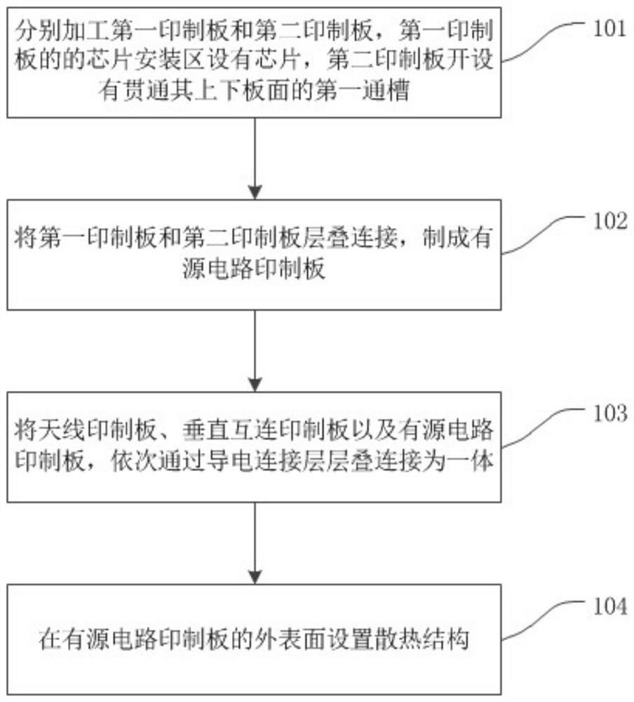
[0035] In order to make the purpose, features and advantages of the present invention more obvious and understandable, the technical solutions in the embodiments of the present invention will be clearly and completely described below in conjunction with the accompanying drawings in the embodiments of the present invention. Obviously, the following The described embodiments are only some, not all, embodiments of the present invention. Based on the embodiments of the present invention, all other embodiments obtained by persons of ordinary skill in the art without making creative efforts belong to the protection scope of the present invention.

[0036] The technical solutions of the present invention will be further described below in conjunction with the accompanying drawings and through specific implementation methods.

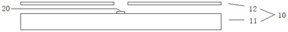
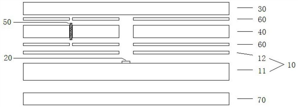
[0037] figure 1 It is a schematic structural diagram of an active circuit printed board 10 provided by an embodiment of the present invention. Such as figur...


PUM


Abstract

The invention relates to the technical field of antennas, and discloses an active circuit printed board, a phased-array antenna and a manufacturing process of the phased-array antenna. The active circuit printed board comprises a first printed board and a second printed board; a chip mounting area is preset on the board surface, facing the second printed board, of the first printed board, and a chip is arranged in the chip mounting area; the second printed board is provided with a first through groove penetrating through the upper and lower board surfaces of the second printed board, and the projection area of the first through groove on the first printed board covers the chip mounting area; and the first printed board on which the chip is attached and the second printed board on which the first through groove is formed are laminated and connected into a whole. The active circuit printed board provided by the embodiment of the invention is formed by laminating and connecting the first printed board on which the chip is pasted in advance and the second printed board on which the through groove is formed in advance, and the through groove design is adopted to replace the traditional blind groove design, so that the processing complexity and the processing difficulty can be reduced, and the higher processing precision can be ensured; the wiring complexity and the chip mounting operation difficulty are reduced, and the processing efficiency is improved.

Description

technical field [0001] The invention relates to the technical field of antennas, in particular to an active circuit printed board, a phased array antenna and a manufacturing process thereof. Background technique [0002] Currently, most antennas, such as phased-array antennas, require the use of active circuit printed boards and other printed boards laminated to form a complete laminated printed board. [0003] Among them, the manufacturing process of the active circuit printed board is as follows: first, press two printed boards with flat surfaces into one to obtain a laminated board; then open a blind groove of a specified depth on the laminated board; finally, in the blind groove Stick the chip. [0004] The manufacturing process and the produced product have the following defects: [0005] The design of the blind slot not only leads to complicated layout and routing of the active board during the design process, but also the manufacturing process of the blind slot itse...

Claims


Application Information

Patent Timeline
IPC IPC(8): H05K1/14H05K1/18H01Q1/00H01Q1/22H01Q1/38H01Q21/00
CPCH05K1/185H05K1/144H01Q1/22H01Q1/38H01Q1/02H01Q21/0087
Inventor 车美娟李松陈皓
Owner CHENGDU TOPANTECH CO LTD
Why Eureka
Try Eureka