
Capacitive coupling circuit device

A technology of capacitive coupling and circuit devices, applied in transmission line coupling devices, near-field transmission systems using capacitive coupling, electrical components, etc., can solve problems such as radiation noise and conduction noise, reduce conduction noise, improve signal quality, The effect of cost cutting

Pending Publication Date: 2021-10-29
PANASONIC INTELLECTUAL PROPERTY MANAGEMENT CO LTD
View PDF1 Cites 0 Cited by
  • Summary
  • Abstract
  • Description
  • Claims
  • Application Information

AI Technical Summary

Problems solved by technology

[0004] However, since the modulated signal transferred from the signal input side through the capacitor is demodulated on the signal output side to regenerate the digital signal, this becomes a noise voltage source and causes conduction noise and radiation noise

Method used


Image

  • Capacitive coupling circuit device
  • Capacitive coupling circuit device
  • Capacitive coupling circuit device

Examples


Embodiment approach 1

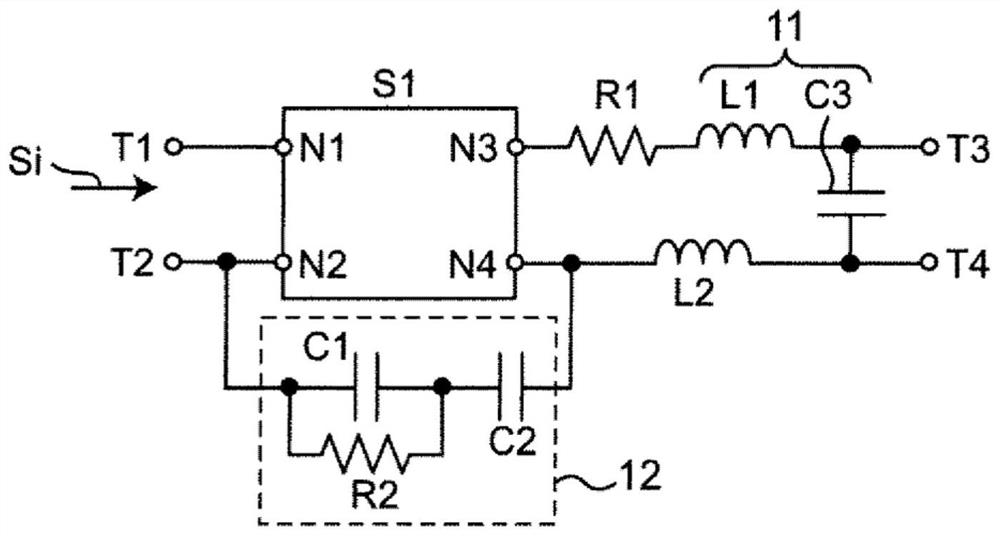
[0036] figure 1 It is a circuit diagram showing a configuration example of the capacitive coupling circuit device according to the first embodiment.

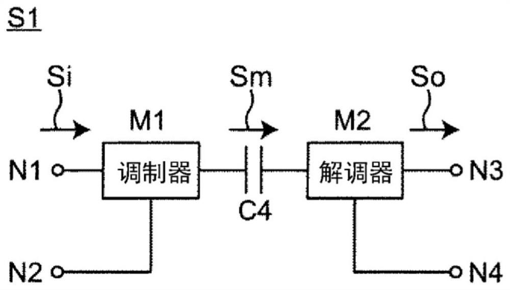
[0037] exist figure 1 Among them, the capacitive coupling circuit device includes external terminals T1 to T4, a capacitive coupling circuit S1, a resistor R1, capacitors C1 to C3, and inductors L1 to L2. Here, the capacitive coupling circuit S1 comprises at least one coupling capacitor C4 (cf. figure 2 ), and has connection terminals N1 to N4. The capacitive coupling circuit device operates, for example, as a communication circuit that outputs an input signal Si input between the external terminals T1 and T2 as an output signal between the external terminals T3 and T4. Here, the external terminals T1 to T4 are provided for the following purposes.

[0038] (1) T1: signal input external terminal;

[0039] (2) T2: the grounding external terminal on the signal input side;

[0040] (3) T3: signal output external terminal;

...

Embodiment approach 2

[0075] Figure 9 It is a circuit diagram showing a configuration example of the capacitive coupling circuit device according to the second embodiment. exist Figure 9 In the capacitive coupling circuit device according to Embodiment 2 and figure 1 Compared with the capacitive coupling circuit device of the present invention, it further includes an inductor L3 connected to the connection terminal N4.

[0076] exist Figure 9 Here, the connection terminal N4 of the capacitive coupling circuit S1 is connected to the external terminal T4 via the inductors L3 and L2. In addition, the connection point of the inductors L3 and L2 is connected to the connection terminal N2 and the external terminal T2 via the ground-side feedback circuit 12 .

[0077] constituted as above Figure 9 The capacitive coupling circuit device with figure 1 Similarly, the capacitive coupling circuit device operates as a communication circuit that outputs a signal input between the external terminals T1 ...


PUM


Abstract

A capacitive coupling circuit device comprises a capacitive coupling circuit that modulates an input signal, subsequently transmits a modulated signal via a coupling capacitor, and then demodulates the modulated signal, wherein the capacitive coupling circuit device comprises a ground-side feedback circuit inserted between a ground terminal at a signal input side of the capacitive coupling circuit and a ground terminal at a signal output side, the ground-side feedback circuit is configured so that a second capacitor is connected in series to a parallel circuit of a first capacitor and a first resistor. Alternatively, the ground-side feedback circuit is configured so that the second capacitor and a third capacitor are serially connected in respective fashion to both ends of the parallel circuit of the first capacitor and the first resistor.

Description

technical field [0001] The present disclosure relates to a capacitive coupling circuit arrangement. Background technique [0002] In in-vehicle equipment, industrial equipment, medical equipment, etc. using high voltage represented by power supply systems of electric vehicles, it is necessary to design to electrically separate (isolate) low-voltage circuits from high-voltage circuits for safety. However, in such a device, signal transmission and reception between a low-voltage circuit and a high-voltage circuit are essential. For example, a high-voltage switching power supply circuit operates upon receiving a control signal from an IC mounted in a low-voltage circuit. In addition, in a high-voltage battery, information on the voltage and temperature of a single battery is received by an IC mounted in a low-voltage circuit, and the received information is fed back to the operation of the power supply system. [0003] In such a device, an isolator is used for signal transmis...

Claims


Application Information

Patent Timeline
Patent Type & Authority Applications(China)
IPC IPC(8): H03H7/52H04B1/10
CPCH03H7/52H04B1/10H04B1/12H04L25/0266H04L25/0294H04B5/22
Inventor 西本太树
Owner PANASONIC INTELLECTUAL PROPERTY MANAGEMENT CO LTD
Learn More