Solid-state imaging device

a solid-state imaging and sensing device technology, applied in the direction of radiation controlled devices, optical radiation measurement, instruments, etc., can solve the adverse effect of thermal noise (ktc noise) due to switching, the effect of reducing the number of counter circuits and reducing the amount of consumed electric power

Active Publication Date: 2013-01-24
HONDA MOTOR CO LTD
View PDF3 Cites 15 Cited by
  • Summary
  • Abstract
  • Description
  • Claims
  • Application Information

AI Technical Summary

Benefits of technology

[0020]According to the present invention, an analog signal, which is representative of energy of light incident on a pixel during the first exposure period, is subtracted from an analog signal, which is representative of energy of light incident on the pixel during the second exposure period. Therefore, a digital value can be produced, which represents the analog signal representative of the energy of light incident on the pixel during the second exposure period minus (−) the analog signal representative of the energy of light incident on the pixel during the first exposure period. In other words, inasmuch as differences between the amounts of photoelectrons in different photoelectron storage units can be calculated upon AD conversion thereof, the number of counter circuits can be reduced, the amount of consumed electric power can be reduced, and noise can be reduced.
[0021]Since the second comparator inverts the signal at a timing later than the timing at which the signal output from the first comparator is inverted, a differential signal can reliably be calculated, which represents the analog signal representative of the energy of light incident on the pixel during the second exposure period minus (−) the analog signal representative of the energy of light incident on the pixel during the first exposure period. Thus, a digital value representing the differential signal an be produced.
[0022]Since the count value produced by the flip-flop circuits is converted into a 1's complement and a 2's complement, the counter circuit, which functions only for counting up pulses, can function as a counter circuit both for counting up and counting down pulses. Since the counter circuit only counts up pulses, the circuit operation thereof is simple, making the switch circuits simple in configuration and reducing the installation area for the counter circuit. Since the count value is expressed as a 2's complement, the count value can easily be handled by digital logic circuits, and addition of a plurality of pixel values using a counter can be coped with.

Problems solved by technology

A distance measuring sensor, which requires the removal of ambient light, is not efficient, in that the distance measuring sensor has to convert the full amount of all of the photoelectrons into a digital signal in order to perform a subsequent subtracting process.
Employing the technology disclosed in Japanese Laid-Open Patent Publication No. 2008-089346, it is difficult to highly integrate pixels, i.e., to achieve higher resolution, because the pixels are combined together with a plurality of switches and capacitors for storing differential photoelectrons.
Further, adverse effect of thermal noise (kTC noise) due to switching may be caused

Method used


Image

  • Solid-state imaging device
  • Solid-state imaging device
  • Solid-state imaging device

Examples


modification 1

(Modification 1)

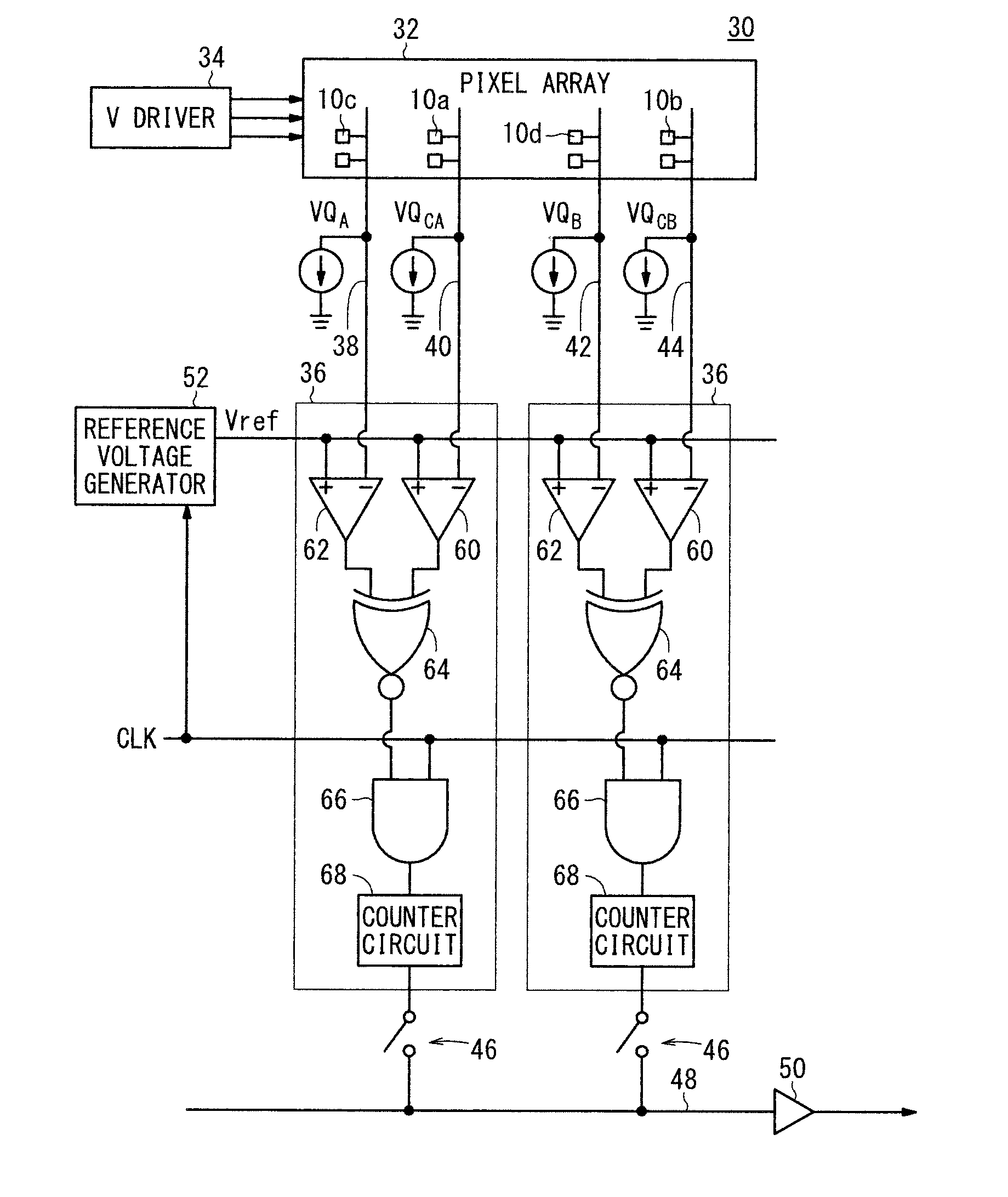
[0138]According to modification 1, the solid-state image sensing device 30 includes an AD converter 90, as shown in FIG. 19, instead of the AD converter 36 shown in FIG. 8. Parts thereof, which have the same functions as those of the AD converter 36 shown in FIG. 8, are denoted by similar reference characters, and such features will not be described below. The AD converter 90 includes a third comparator 100, a judging circuit 102, and a complement control circuit 104, in addition to the first comparator 60, the second comparator 62, the differential circuit 64, the AND circuit 66, and the counter circuit 68.

[0139]The third comparator 100 compares the first analog signal VQCA or VQCB, which is output from the first pixel 10a or 10b, with the second analog signal VQA or VQB, which is output from the second pixel 10c or 10d. The second analog signal VQA or VQB is input to the positive terminal of the third comparator 100, whereas any one of the first analog signal VQCA ...

modification 2

(Modification 2)

[0163]In the above embodiment, the first analog signals VQCA, VQCB and the second analog signals VQA, VQB are obtained from different first pixels 10a, 10b and different second pixels 10c, 10d, respectively. According to modification 2, however, the first analog signals VQCA, VQCB and the second analog signals VQA, VQB are obtained from one pixel.

[0164]According to modification 2, a unit pixel (hereinafter referred to simply as a pixel) 108 is used instead of the pixel 10 shown in FIGS. 2 through 7. The pixel 108 comprises a photodetector 110, capacitors C10 through C13, switching elements SW10 through SW22, an FD 112, a photoelectron discharger 114, a pixel amplifier 116, an FD 118, a photoelectron discharger 120, a pixel amplifier 122, an FD 124, a photoelectron discharger 126, a pixel amplifier 128, an FD 130, a photoelectron discharger 132, and a pixel amplifier 134.

[0165]The capacitors C10 through C13 are connected respectively to the photodetector 110 through t...

modification 3

(Modification 3)

[0174]FIG. 28 is a diagram showing an arrangement of a solid-state image sensing device 30 according to a third modification. Parts thereof, which have the same functions as those shown in FIG. 8, are denoted by identical reference characters. According to modification 3, an AND circuit 140 and a counter circuit (second counter circuit) 142 are added to the solid-state image sensing device 30 shown in FIG. 8. The AND circuit 140 has the same function as the AND circuit 66, and the counter circuit 142 has the same function as the counter circuit 68, i.e., to convert the count value into a 2's complement. A signal that depends on the first analog signal VQCB output from the first comparator 60 is input to the differential circuit 64 and to the additional AND circuit 140. A clock signal also is input to the AND circuit 140. The additional AND circuit 66 outputs a pulse train to the counter circuit 142, which depends on the first analog signal VQCB output from the first ...


PUM


Abstract

Disclosed is a solid-state imaging device capable of calculating the difference in charge obtained by photoelectric conversion, and capable of a high level of integration. A solid-state imaging device is provided with an AD converter which is provided with: a first comparator which outputs a signal corresponding to a first analogue signal of a first pixel by comparing said first analogue signal with a reference voltage supplied from the reference voltage generation unit which generates a reference voltage which gradually changes; a second comparator which outputs a signal corresponding to a second analogue signal of a second pixel by comparing said second analogue signal with the reference voltage supplied by the reference voltage generation unit; a difference circuit which finds the difference between the signal corresponding to said first analogue signal and the signal corresponding to said second analogue signal and outputs a difference signal; and a counter circuit which counts the number of pulses in a pulse sequence corresponding to the aforementioned difference signal and converts said difference signal into a digital signal.

Description

TECHNICAL FIELD[0001]The present invention relates to a solid-state image sensing device (solid-state imaging device) that functions as a distance measuring sensor.BACKGROUND ART[0002]Heretofore, in the field of CMOS image sensors, there has been known a column ADC technology for obtaining AD conversion results, which are resistant to exogenous noise.[0003]Japanese Laid-Open Patent Publication No. 09-238286 discloses that an amplifying solid-state image sensing device, which incorporates a plurality of analog-to-digital converters with a noise reducing function (integrating analog-to-digital converters) therein, latches and then successively selects digital signals from the analog-to-digital converters.[0004]Heretofore, there has also been known a TOF (Time Of Flight) method for measuring the distance up to a subject by detecting light reflected from a subject that is illuminated by an illuminating unit. Since pixels, which detect the reflected light, also receive ambient light such...

Claims


Application Information

Patent Timeline
Patent Type & Authority Applications(United States)
IPC IPC(8): H01L27/146
CPCH03M1/123H03M1/56H04N5/378H04N5/361H04N5/335H04N25/00H04N25/63H04N25/75
Inventor KOREKADO, KEISUKEKAMIYAMA, TOMOYUKINISHIMURA, YOICHI
Owner HONDA MOTOR CO LTD
Why Eureka
Try Eureka