Preparation method of low-trigger and low-capacitance chip type electrostatic suppressor

An electrostatic suppression and low triggering technology, applied in the direction of protection against damage caused by electrostatic discharge, electric solid devices, circuits, etc., can solve problems such as low capacitance

Pending Publication Date: 2021-11-05
SEMITEL ELECTRONICS
View PDF1 Cites 0 Cited by
  • Summary
  • Abstract
  • Description
  • Claims
  • Application Information

AI Technical Summary

Problems solved by technology

[0005] Aiming at the deficiencies of the prior art, the present invention provides a method for preparing a low-trigger, low-capacity chip electrostatic suppressor. The electrode gap prepared by laser precision cutting has the same gap width as compared with the electrode prepared by the thick film printing process. Good performance, using double-slit electrode design to achieve low capacitance, which solves the problem of ultra-small capacitance, using 3-layer laminated board design to achieve a higher density of the internal structure, with high anti-permeation and moisture resistance performance, can effectively solve the problems in the background technology

Method used


Image

  • Preparation method of low-trigger and low-capacitance chip type electrostatic suppressor

Examples


preparation example Construction

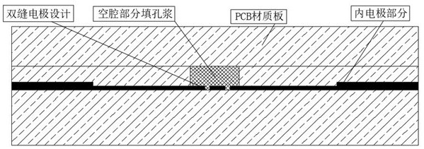
[0026] Such as figure 1 As shown, a preparation method of a low-trigger, low-capacity chip electrostatic suppressor comprises the following steps:

[0027] S1: Slurry selection: A combination of nano-material preparation technology, semiconductor materials, polymer materials and PCB board technology is used to print a functional material layer with a loose skeleton structure and semiconductor characteristics on the electrode grooving part. There are sharp edges and The functional paste is a gap formed by a loose skeleton structure to achieve low voltage characteristics;

[0028] S2: Laser cutting: the electrode gap prepared by laser precision cutting, the width of the gap is controlled, and the electrode is prepared through the copper clad laminate to combine with the substrate to ensure the triggering performance of the device and provide a convenient channel for electron transmission;

[0029] S3: Double slit design: use double slit cutting electrode, the cutting slit is 12~1...

Embodiment 1

[0040] The width of the slit in the step S2 is controlled to be 13um, and the sum of the slit widths of the double slits is 28um.

[0041] In step S3, the electrode is cut with a double slit design, and the cut slit is 13um.

[0042] In step S2, on the basis of ensuring no leakage, the device minimizes the trigger voltage to 280V and the operating voltage to 2KV to achieve better ESD responsiveness.

[0043] In step S3, a double-slit electrode design is used to achieve low capacitance, which solves the problem of ultra-small capacitance, and the capacitance is reduced from the existing 0.15pf to 0.07pf.

Embodiment 2

[0045] The width of the slit in the step S2 is controlled to be 14um, and the sum of the slit widths of the double slits is 29um.

[0046] In step S3, the electrode is cut with a double slit design, and the cut slit is 14um.

[0047] In step S2, on the basis of ensuring no leakage, the device minimizes the trigger voltage to 290V and the operating voltage to 2KV to achieve better ESD responsiveness.

[0048] In step S3, a double-slit electrode design is used to achieve low capacitance and solve the problem of ultra-small capacitance. The capacitance is reduced from the existing 0.15pf to 0.071pf.

[0049] Working principle: Combining nano-material preparation technology, semiconductor materials, polymer materials and PCB board technology, printing a functional material layer with a loose skeleton structure and semiconductor characteristics on the electrode grooving part, and there are sharp and functional pastes in the grooving part of the electrode The gap formed by the loos...


PUM


Abstract

The invention discloses a preparation method of a low-trigger and low-capacitance chip type electrostatic suppressor. The method comprises the following operation steps of printing a functional material layer with a loose skeleton structure and semiconductor characteristics at an electrode grooving part by combining a nano material preparation technology, a semiconductor material technology, a high polymer material technology and a PCB technology. The electrode grooving part has a gap formed by the tip and the functional slurry as a loose skeleton structure, so that the low-voltage characteristic is realized, and the prepared electrode gap is precisely cut by laser. According to the preparation method of the low-trigger and low-capacitance chip type electrostatic suppressor, compared with an electrode prepared through a thick film printing process, the electrode gaps prepared through laser precision cutting are good in gap width consistence; the double-gap electrode design is adopted, so that the low capacitance value is achieved, and the problem of ultra-small capacitance value is solved; by adopting the three-layer pressing plate design, the higher density of the internal structure is achieved, and the higher anti-permeation and moisture-resistant performance is achieved.

Description

technical field [0001] The invention relates to the technical field of electrostatic protection, in particular to a preparation method of a low-trigger, low-capacity chip-type electrostatic suppressor. Background technique [0002] The preparation method of the electrostatic suppressor is a method of processing and manufacturing the chip electrostatic suppressor. The electrostatic protector is suitable for resisting ESD and other voltage mutation pulses. The device can protect up to 18 data channels and can resist the peak pulse of 30kV at most. . Its pin capacitance is only 10pF, which is very suitable for protecting high-speed or high-frequency (up to 200MHz or more) data lines. Due to their small size and very small leakage current, they are very suitable for some applications that have strict requirements on space and power consumption. In some occasions, with the continuous development of science and technology, people have higher and higher requirements for the manufac...

Claims


Application Information

Patent Timeline
Patent Type & Authority Applications(China)
IPC IPC(8): H05K9/00H01L23/60
CPCH05K9/0067H01L23/60
Inventor 董福兴戴剑仇利民崔海周郭志军
Owner SEMITEL ELECTRONICS
Why Eureka
Try Eureka