Waveform generation and acquisition method and device based on FPGA

A technology of waveform generation and acquisition method, applied in the field of electronic science, can solve the problems of high design cost, complex circuit, unfavorable cost saving, etc., and achieve the effect of simplifying design and saving design cost

Pending Publication Date: 2021-11-09
中国兵器装备集团自动化研究所有限公司
View PDF0 Cites 0 Cited by
  • Summary
  • Abstract
  • Description
  • Claims
  • Application Information

AI Technical Summary

Problems solved by technology

[0005] The technical problem to be solved by the present invention is that the existing waveform generation and acquisition methods require complex circuit design and higher design costs to process simple waveform generation and acquisition, which is not conducive to cost saving. The purpose is to provide a waveform based on FPGA Generation and collection method and device to solve the above problems

Method used


Image

  • Waveform generation and acquisition method and device based on FPGA
  • Waveform generation and acquisition method and device based on FPGA
  • Waveform generation and acquisition method and device based on FPGA

Examples


Embodiment

[0048] The signal that the present invention is suitable for input and output is a square wave signal with constant level.

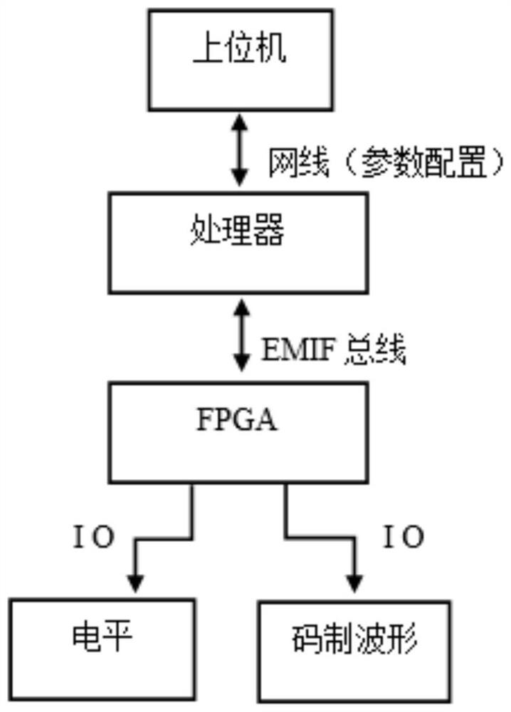
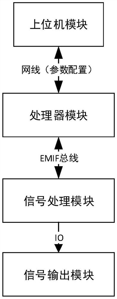
[0049] The functional circuit of the FPGA-based waveform generation and acquisition method designed by the present invention is composed of an FPGA chip, a gate circuit and a processor. It is suitable for circuits that need to generate a wider square wave code system and input a wider square wave code system waveform (code system width ≥ 1ms).

[0050] When the waveform is generated, when the processor receives the control command from the host computer, the processor writes the relevant instructions or parameters of the coded waveform or level to be generated by each signal to the FPGA through the EMIF bus. The FPGA generates corresponding coded waveforms or level signals according to the instructions.

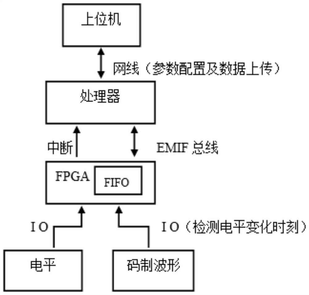
[0051] When the waveform is collected, the FPGA completes the signal collection and information upload according to the relevant instructions of the s...


PUM


Abstract

The invention discloses a waveform generation and acquisition method and device based on an FPGA. The device comprises an upper computer module, a processor module, a signal processing module and a signal output module. The upper computer module is used for receiving a waveform generation control instruction and parameters input by a user and sending the waveform generation control instruction and parameters to the processor module; the processor module is used for processing the waveform generation control instruction and parameters to obtain first processing data and then sending the first processing data to the signal processing module; the signal processing module is used for determining the type of a signal to be output according to the first processing data and sending the signal type to the signal output module; the signal output module is used for outputting waveform signals according to the signal types. In a circuit for generating a wider square wave code system waveform and inputting the wider square wave code system waveform, the function of processing a square wave signal by AD and DA can be replaced, the design of the circuit is simplified, and waveform generation and acquisition are realized on the basis of saving the design cost.

Description

technical field [0001] The invention relates to the field of electronic science and technology, in particular to an FPGA-based waveform generation and acquisition method and device. Background technique [0002] In practical engineering applications, if the AD chip is used to achieve signal acquisition, the peripheral circuit of the AD chip needs to be designed, and a processor or FPGA is required to configure the AD chip, and finally the AD chip is used to collect the input signal: ①If it is FPGA configuration AD chip, then the AD chip sends the collected signal to the FPGA, and the FPGA transmits the data to the processor, and finally transmits the data to the upper computer for drawing. ②If the processor is equipped with an AD chip, then the AD chip will send the collected signal to the processor, and finally transmit the data to the upper computer for drawing. [0003] If the DA chip is used to realize signal generation, the peripheral circuit of the DA chip needs to be...

Claims


Application Information

Patent Timeline
IPC IPC(8): G06F1/02G06F15/78H03K3/02H03K5/01
CPCG06F1/022G06F15/7807H03K3/02H03K5/01
Inventor 张自圃邵雨新李坤贺吴昌昊李中
Owner 中国兵器装备集团自动化研究所有限公司
Why Eureka
Try Eureka