Printed circuit board copper embedding device and printed circuit board processing method

A technology of printed circuit boards and circuit boards, which is applied in the direction of circuit heating devices, printed circuit manufacturing, printed circuits, etc., can solve problems affecting production efficiency, printed circuit board damage, and product quality, and achieve the goal of reducing clamping time, avoiding inaccurate positioning, and convenient and fast clamping

Active Publication Date: 2021-11-09
四川英创力电子科技股份有限公司
View PDF10 Cites 4 Cited by
  • Summary
  • Abstract
  • Description
  • Claims
  • Application Information

AI Technical Summary

Problems solved by technology

[0002] At present, in order to enhance the heat dissipation performance of the printed circuit board, copper blocks are embedded in the printed circuit board, but because the installation position of the copper block on the printed circuit board is uncertain and irregular, the copper block is generally placed manually. Embedding in the square hole, and then injecting resin, but this greatly affects the production efficiency, and affects the yield rate. In the prior art, there is also a method without injecting resin, directly pressing the copper block into the square hole of the printed circuit board , the size of the copper block used in this method is larger than the size of the square hole, which is easy to cause damage to the printed circuit board and affect the product quality

Method used


Image

  • Printed circuit board copper embedding device and printed circuit board processing method
  • Printed circuit board copper embedding device and printed circuit board processing method
  • Printed circuit board copper embedding device and printed circuit board processing method

Examples


Embodiment approach

[0054] The specific implementation is described as follows:

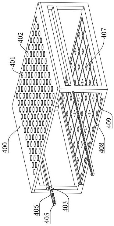
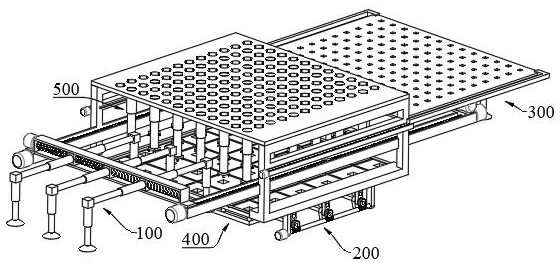
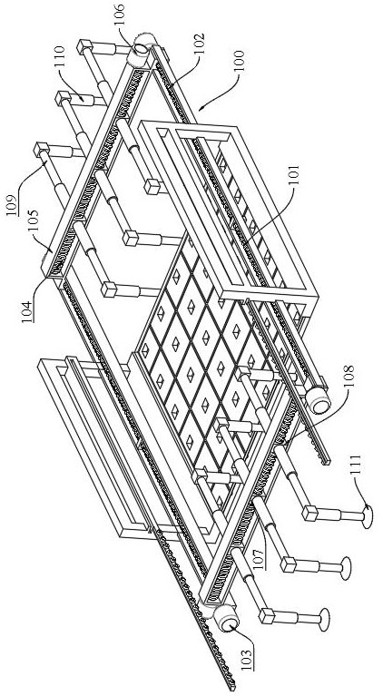
[0055] Wherein the method for using the printed circuit board embedded copper block device used in step 3 is to select different limit strips 409 according to the size of the printed circuit board, and connect the four limit strips 409 end to end to make one limit strip The second locking pin 411 on the 409 cooperates with the second locking groove 412 of another adjacent limiting bar 409 to form a limiting area, and the combined limiting bar 409 is placed on the bottom of the support frame 400, so that The boss 410 cooperates with the mounting groove 408; the first telescopic rod 109 is started to adjust the distance between the second telescopic rods 110 on both sides of the second screw mandrel 104, and the second motor 106 is started to drive the second screw mandrel 104 to rotate. The two sections of thread of the second screw mandrel 104 rotate in the opposite direction, so that the connecting blocks 108 can m...


PUM


Abstract

The invention provides a printed circuit board copper embedding device and a printed circuit board processing method. The device comprises a transfer mechanism, a jacking mechanism, a bearing mechanism, a supporting frame and a clamping mechanism. The supporting frame is used for bearing a printed circuit board. The transfer mechanism comprises two sets of transfer assemblies which are symmetrically arranged and used for transferring the printed circuit board, and the jacking mechanism is arranged below the supporting frame and used for jacking the printed circuit board to a preset height. The bearing mechanism is fixed to the supporting frame and used for loading the copper block to the position below the clamping mechanism. The clamping mechanism comprises a plurality of clamping assemblies and is used for clamping copper blocks into square holes of the printed circuit board. The printed circuit board processing method comprises the following steps: manufacturing a circuit board; manufacturing a copper block; clamping the copper block into the square hole of the circuit board; injecting resin; flattening the circuit board; performing press fit; performing electroplating; drilling holes; and performing copper deposition. The printed circuit board copper embedding device is simple in structure, adapts to the requirements of different printed circuit board sizes, can avoid inaccurate positioning, is convenient to clamp, shortens the production time, and improves the production efficiency.

Description

technical field [0001] The invention relates to the technical field of printed circuit board production and processing, in particular to a printed circuit board copper embedding device and a printed circuit board processing method. Background technique [0002] At present, in order to enhance the heat dissipation performance of the printed circuit board, copper blocks are embedded in the printed circuit board, but because the installation position of the copper block on the printed circuit board is uncertain and irregular, the copper block is generally placed manually. Embedding in the square hole, and then injecting resin, but this greatly affects the production efficiency, and affects the yield rate. In the prior art, there is also a method without injecting resin, directly pressing the copper block into the square hole of the printed circuit board , The size of the copper block used in this method is larger than the size of the square hole, which is easy to cause damage t...

Claims


Application Information

Patent Timeline
Patent Type & Authority Applications(China)
IPC IPC(8): H05K3/00H05K1/02H05K3/46
CPCH05K3/00H05K1/0201H05K3/4611H05K2201/06H05K2203/061
Inventor 张仁军李清华林涛胡志强牟玉贵
Owner 四川英创力电子科技股份有限公司
Why Eureka
Try Eureka