Supercharge Your Innovation With Domain-Expert AI Agents!

Chip, chip production method and electronic device

A chip and particle technology, applied in the field of chip preparation, can solve the problems of poor chip reliability and increased forward voltage drop, and achieve the effects of enhancing stability, reducing separation distance, and improving use adaptability

Pending Publication Date: 2021-11-12
GREE ELECTRIC APPLIANCES INC +1
View PDF6 Cites 0 Cited by
  • Summary
  • Abstract
  • Description
  • Claims
  • Application Information

AI Technical Summary

Problems solved by technology

[0003] In order to solve the technical problems of increased forward conduction voltage drop and poor reliability of the chip caused by the voltage foldback phenomenon in the chip, the main purpose of this application is to provide a chip that can reduce the voltage foldback phenomenon in the chip and improve the reliability of the chip. Chip preparation method and electronic device

Method used


Image

  • Chip, chip production method and electronic device
  • Chip, chip production method and electronic device
  • Chip, chip production method and electronic device

Examples


Embodiment Construction

[0043] In order to make the purposes, technical solutions and advantages of the embodiments of the present application clearer, the technical solutions in the embodiments of the present application will be clearly and completely described below in conjunction with the drawings in the embodiments of the present application. Obviously, the described embodiments It is a part of the embodiments of this application, but not all of them. Based on the embodiments in the present application, all other embodiments obtained by persons of ordinary skill in the art without making creative efforts belong to the protection scope of the present application.

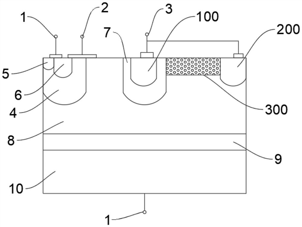
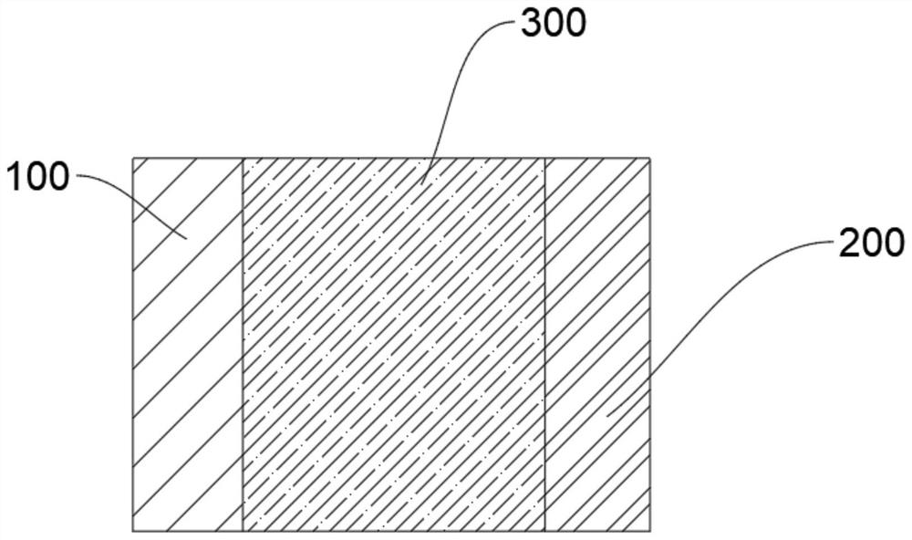
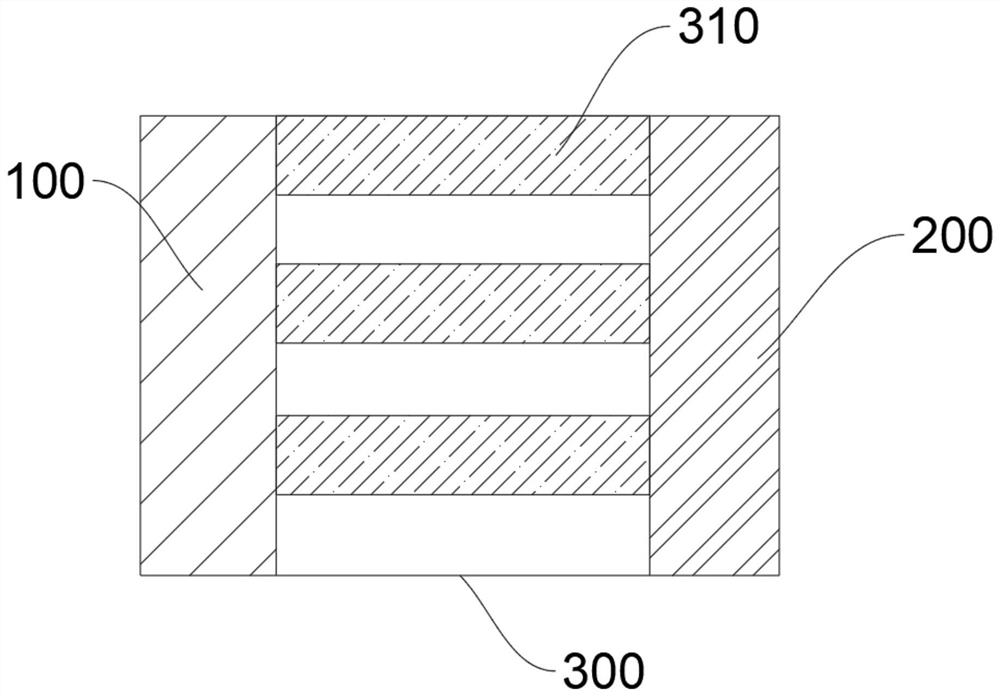
[0044] The traditional method to eliminate the voltage foldback phenomenon is to increase the flow resistance RB of electrons between the anode 3P+ and the anode 3N+, which can be achieved by increasing the distance between the anode 3P+ and N+, so that it is more difficult for the electrons to be collected by the anode N+ region, and th...


PUM


Abstract

The invention relates to the technical field of chip production, and discloses a chip, a chip production method and an electronic device. The chip comprises a substrate layer, a buried oxide layer and an N-type drift layer, the N-type drift layer comprises a first side close to the substrate layer and a second side away from the substrate layer, a first anode region and a second anode region are formed on the second side, and a dielectric region is formed between the first anode region and the second anode region. And the dielectric region comprises point defects which are densely distributed and formed on the N-type drift layer. Compared with the prior art, the resistance in the dielectric region is improved by forming the point defect in the dielectric region so that the movement of electrons between the first anode region and the second anode region is inhibited, the voltage turn-back phenomenon of the chip is weakened, and the overall stability of the chip is improved.

Description

technical field [0001] The present application relates to the technical field of chip preparation, in particular to a chip, a chip preparation method and an electronic device. Background technique [0002] Due to the low conduction voltage drop of bipolar transistors and the high input resistance and high-speed switching of field effect transistors, IGBTs have become mainstream devices in the field of high-frequency power switching devices, and are widely used in transportation, smart grid and many other fields. Traditional IGBT devices cannot be turned on in the reverse state. Generally, a fast recovery diode (FRD) needs to be connected in parallel for freewheeling protection. However, this will increase additional packaging cost and area. The reverse conduction insulated gate bipolar transistor (RC IGBT) solves the packaging problem of both by integrating IGBT and FRD on the same cell, and has the advantages of small device size, high current density, and low packaging co...

Claims


Application Information

Patent Timeline
IPC IPC(8): H01L29/06H01L29/739H01L21/331
CPCH01L29/7393H01L29/0684H01L29/66325
Inventor 葛孝昊肖婷林苡任史波
Owner GREE ELECTRIC APPLIANCES INC
Features
  • R&D
  • Intellectual Property
  • Life Sciences
  • Materials
  • Tech Scout
  • Unparalleled Data Quality
  • Higher Quality Content
  • 60% Fewer Hallucinations
Learn More