

Automatic gain control circuit and method of transimpedance amplifier circuit
An automatic gain control and transimpedance amplifier technology, applied in the field of optoelectronic communication, can solve the problems such as the inability of the transimpedance gain to remain stable, the long convergence time of the automatic gain control loop, and the jitter of the output signal, so as to improve the input dynamic range and widen the dynamic range. Good scope and scalability
- Summary
- Abstract
- Description
- Claims
- Application Information
AI Technical Summary
Problems solved by technology
Method used
Image

Examples
Embodiment 1
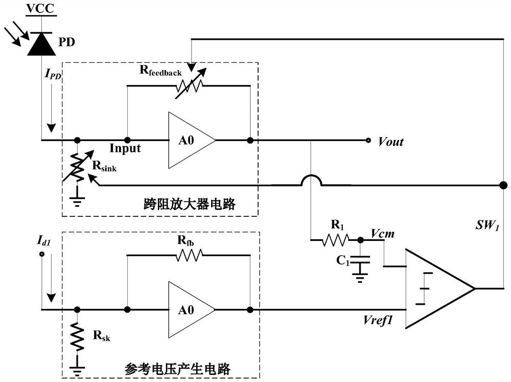
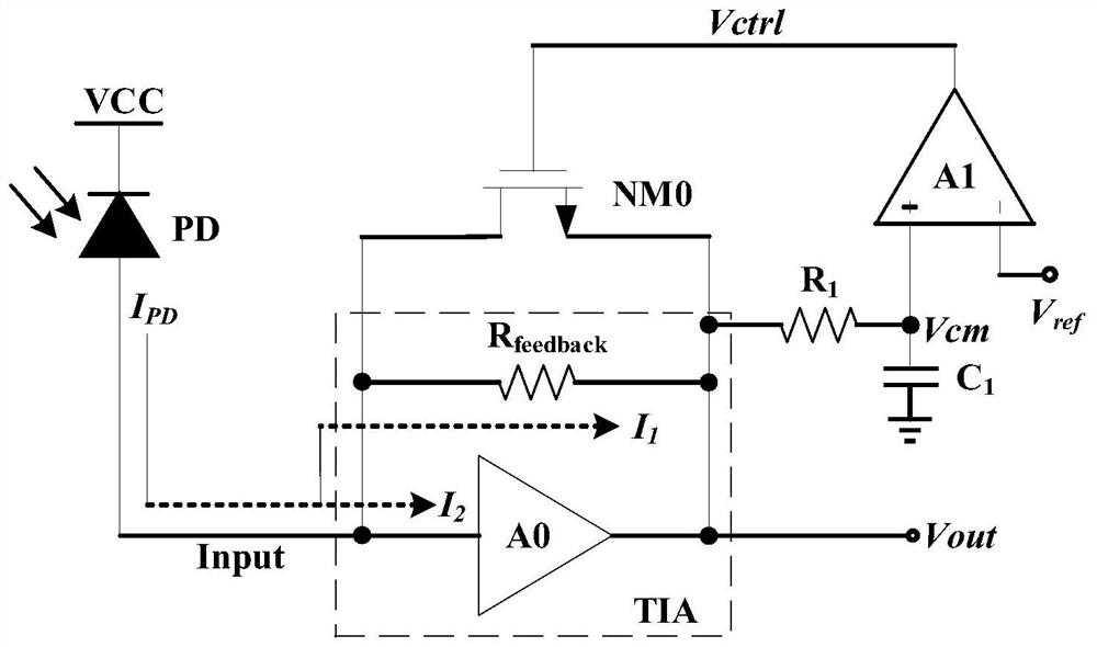
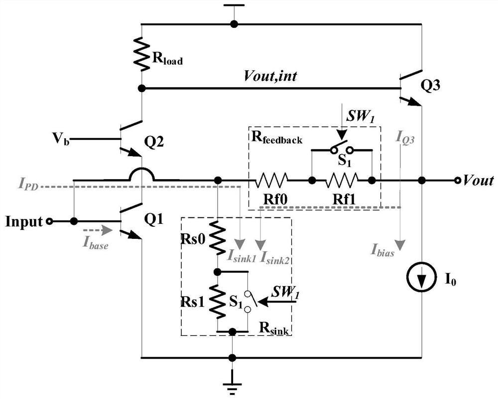
[0038] refer to figure 1 , the embodiment of the present invention provides an automatic gain control circuit of a transimpedance amplifier circuit, on the basis of Embodiment 1, wherein, refer to image 3 , transimpedance amplifier circuit, including gm amplifier tube Q1, cascode tube Q2, load circuit R load , emitter follower Q3, emitter follower bias current source I 0 , Feedback resistor R feedback , input bias resistor R sink . where the feedback resistor R feedback A resistor Rf0, a resistor Rf1, and a switch S connected in parallel with the resistor Rf1 1 Composition; input bias resistor R sink It consists of a resistor Rs0, a resistor Rs1, and a switch S1 connected in parallel with the resistor Rs1. R feedback and R sink Switch S in 1 It can be realized by a transmission gate composed of NMOS or NMOS and PMOS in parallel.
[0039] image 3 In the transimpedance amplifier circuit, the Input voltage at the input terminal is clamped at the V of Q1 be , flows...
Embodiment 2
[0046] refer to figure 1 , the embodiment of the present invention provides an automatic gain control circuit of a transimpedance amplifier circuit, on the basis of Embodiment 1, wherein, refer to Figure 4 , transimpedance amplifier circuit, and increase the second reference voltage generation circuit, input current I d2 , latching comparator and output digital control bit SW 2 , which can widen the dynamic range. Hypothesis I d1 d2 , the threshold current for gain control switching of the transimpedance amplifier is N×I d1 , N×I d2 . When I PD d1 , the digital control bit output by the first latch comparator is low level SW 1 =0, the digital control bit output by the second latch comparator is low level SW 2 =0, the feedback resistor R feedback The resistance is Rf0+Rf1+Rf2, the input bias resistor R sink The resistance is Rs0+Rs1+Rs2; when I d1 ≤I PD d2 , the digital control bit output by the first latch comparator is high level SW 1 =1, the digital control bi...
PUM
 Abstract
Description
Claims
Application Information