Manufacturing method of TEOS film

A manufacturing method and thin-film technology, applied in semiconductor/solid-state device manufacturing, gaseous chemical plating, coating, etc., can solve the problem of easy delamination of TEOS film, and achieve lower leakage current, better adhesion, and improved compactness. Effect

Active Publication Date: 2021-11-19
BETONE TECH SUZHOU INC
View PDF5 Cites 0 Cited by
  • Summary
  • Abstract
  • Description
  • Claims
  • Application Information

AI Technical Summary

Problems solved by technology

[0003] The purpose of this application is to provide a method for making a TEOS film, so as to i

Method used


Image

  • Manufacturing method of TEOS film
  • Manufacturing method of TEOS film

Examples


Embodiment Construction

[0026] In order to make the purpose, technical solutions and advantages of the embodiments of the present application clearer, the technical solutions in the embodiments of the present application will be clearly and completely described below. Those who do not indicate the specific conditions in the examples are carried out according to the conventional conditions or the conditions suggested by the manufacturer. The reagents or instruments used were not indicated by the manufacturer, and they were all conventional products that could be purchased from the market.

[0027] The characteristics and performance of the present application will be described in further detail below in conjunction with the examples.

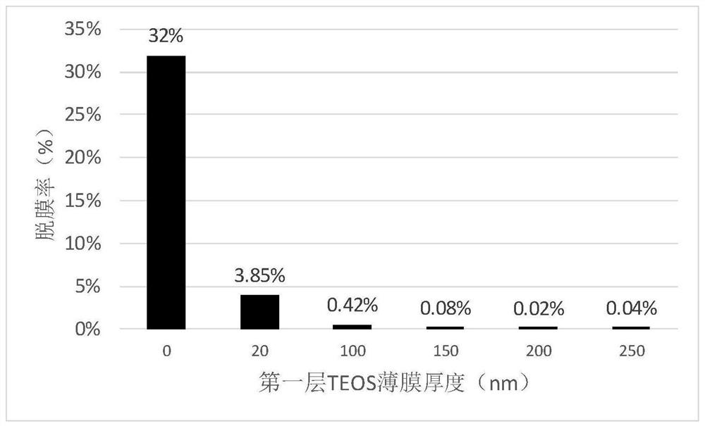
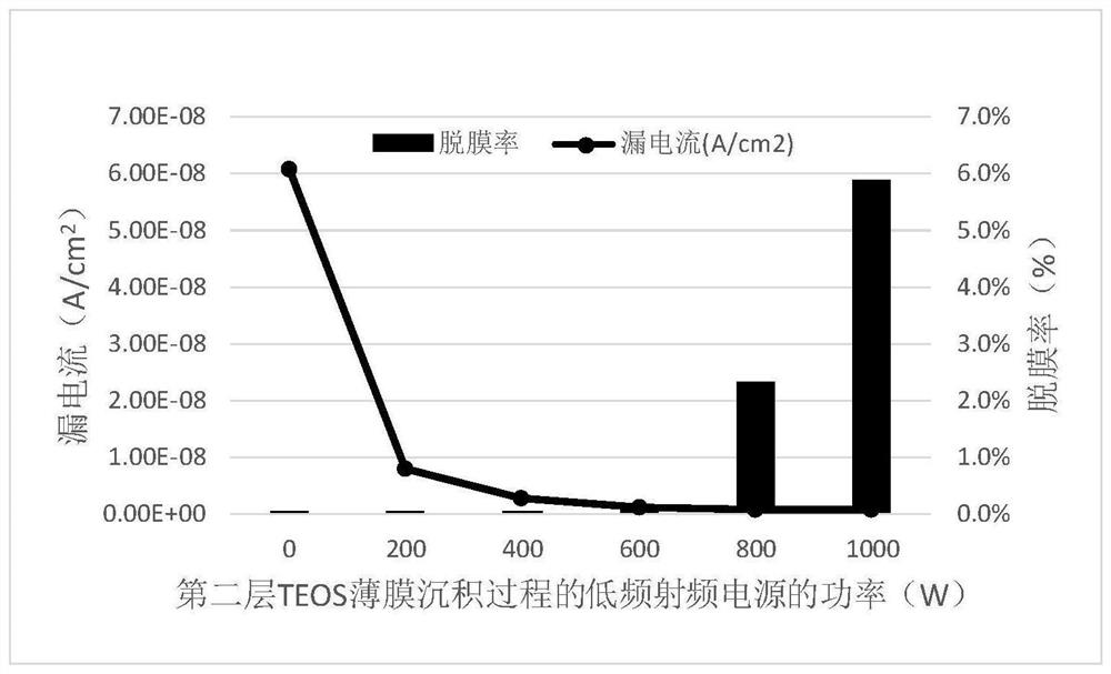
[0028] In the field of semiconductors, related technologies use chemical vapor deposition to produce TEOS films. In order to promote the reaction and improve the insulation performance of TEOS films, low-frequency radio frequency power is used to ionize the raw material...


PUM


Abstract

The invention discloses a manufacturing method of a TEOS film, and relates to the technical field of semiconductors. The method comprises the steps that a first layer of TEOS film is deposited on a silicon wafer, a second layer of TEOS film is deposited on the first layer of TEOS film, a low-frequency radio-frequency power source is not adopted for ionization in the deposition process of the first layer of TEOS film, and a low-frequency radio-frequency power source is adopted for ionization in the deposition process of the second layer of TEOS film. The thickness of the first layer of TEOS film is 20-400 nm, and the thickness of the second layer of TEOS film is 2000-6000 nm. The first layer of TEOS film has lower pressure stress, so that the adhesive force between the first layer of TEOS film and the silicon wafer is stronger, and the film is not easy to release. The second layer of TEOS film has better compactness, so that the leakage current is reduced. Therefore, the TEOS film prepared by adopting the preparation method provided by the invention not only keeps relatively good insulating properties but also is not easy to fall off from the silicon wafer.

Description

technical field [0001] The present application relates to the field of semiconductor technology, in particular, to a method for manufacturing a TEOS film. Background technique [0002] Integrated circuit chip packaging through-silicon via technology (TSV) is the key technology to realize 2.5D / 3D multi-chip stacking and chip heterogeneous integration. TSV involves many key technologies, such as through hole etching, deposition of insulating layer in the hole, electroplating and chip thinning, etc. Among them, the deposition of the insulating layer is an extremely important link, and its main function is to prevent the formation of conductive channels between the upper interconnection metal wiring and the chip surface metal and silicon substrate. Because the TEOS film (Tetraethylorthosilicate) obtained by chemical vapor deposition has good step coverage and low-temperature deposition characteristics (100 ° C ~ 200 ° C), it is usually used as an insulating layer for through-si...

Claims


Application Information

Patent Timeline
IPC IPC(8): C23C16/44C23C16/02C23C16/505H01L21/02
CPCC23C16/44C23C16/505C23C16/0272H01L21/02123H01L21/02274
Inventor 方合宋维聪
Owner BETONE TECH SUZHOU INC
Why Eureka
Try Eureka