Unlock instant, AI-driven research and patent intelligence for your innovation.

Negative capacitance L-shaped gate tunneling field effect transistor and preparation method thereof

A technology of tunneling field effect and negative capacitance, which is applied in semiconductor/solid-state device manufacturing, circuits, electrical components, etc. It can solve the problems of limited improvement of device characteristics, difficulty in increasing the tunneling probability of LG-TFET, etc., and increase the channel surface The effect of electric potential, large band-to-band tunneling rate, and large on-state current

Pending Publication Date: 2021-11-19
XIDIAN UNIV
View PDF12 Cites 0 Cited by
  • Summary
  • Abstract
  • Description
  • Claims
  • Application Information

AI Technical Summary

Problems solved by technology

[0003] However, limited by the innovation of the device structure and the diversity of heterogeneous materials, the improvement of device characteristics is limited, and the tunneling probability of the traditional L-channel tunneling field effect transistor LG-TFET is difficult to increase

Method used


Image

  • Negative capacitance L-shaped gate tunneling field effect transistor and preparation method thereof
  • Negative capacitance L-shaped gate tunneling field effect transistor and preparation method thereof
  • Negative capacitance L-shaped gate tunneling field effect transistor and preparation method thereof

Examples


Embodiment Construction

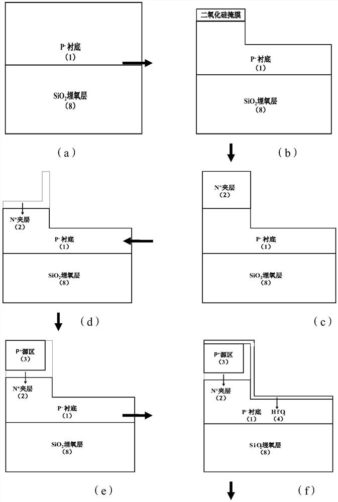
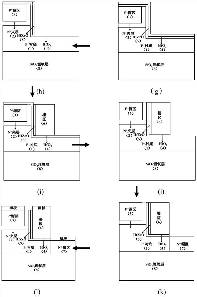
[0042] Embodiments of the present invention will be described in detail below in conjunction with examples, but those skilled in the art will understand that the following examples are only used to illustrate the present invention, and should not be considered as limiting the scope of the present invention.

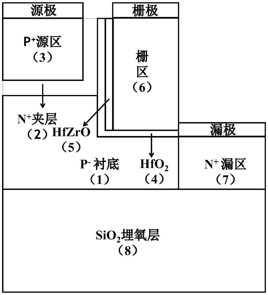
[0043] refer to figure 1 , is a negative capacitance L-type gate tunneling field effect transistor of the present invention, comprising: a P-substrate 1, a P+-type source region 3, a gate region 6, and a drain region 7, wherein, the bottom of the P-substrate 1 is provided with Buried oxide layer 8, N+ type interlayer 2 is deposited on the upper left part of the P-substrate 1, a lower step is etched on the right side of the P-substrate 1, and the drain region 7 is located on the upper part of the lower step, and its thickness is the same as that of the P-substrate 1 same;

[0044] An upper step is etched on the N+ type interlayer 2, a P+ type source region 3 is deposited ...


PUM

PropertyMeasurementUnit
heightaaaaaaaaaa
lengthaaaaaaaaaa
thicknessaaaaaaaaaa

Abstract

The invention belongs to the technical field of microelectronic devices, and discloses a negative capacitance L-shaped gate tunneling field effect transistor and a preparation method thereof. The negative capacitance L-shaped gate tunneling field effect transistor comprises a buried oxide layer, a P-substrate, an N + type interlayer, a P + type source region, a gate oxide layer medium, a ferroelectric medium layer, a gate region and a drain region; the P + type source region and the N + type interlayer are located in the upper left portion of the P-substrate from top to bottom, the gate oxide layer medium is located in the right side of the N + type interlayer, the gate region is located on the gate oxide layer, the drain region is located on the right portion of the P-substrate, and the buried oxide layer is located below the P-substrate. A metal / / Hf0.5Zr0.5O / HfO2 / Si stacked structure is formed in the left side of the P + source region, so that the grid control capability is improved, the channel surface potential is increased, and the on-state current of the tunneling field effect transistor TFET is improved; and the N + interlayer and the P + source region are generated in the left side of the gate region, the tunneling area is increased, and line tunneling is expected to be formed.

Description

technical field [0001] The invention relates to the technical field of microelectronic devices, in particular to a negative capacitance L-type gate tunneling field effect transistor and a preparation method thereof, which can be used in the preparation of large open current and low power consumption electronic devices. Background technique [0002] In the process of continuous miniaturization of complementary MOS technology, adjusting the power supply voltage is the most effective way to reduce power consumption. However, taking this approach in nanoscale circuits will no longer be feasible. A low threshold voltage causes a drastic increase in device leakage current, further increasing the static power consumption of the device. As a breakthrough, tunneling field-effect transistor TFET with gate-controlled reverse-biased p-i-n diode structure has become one of the candidates for next-generation low-power devices due to its low leakage current and steep subthreshold slope. ...

Claims


Application Information

Patent Timeline
Patent Type & Authority Applications(China)
IPC IPC(8): H01L29/739H01L29/51H01L29/06H01L21/331
CPCH01L29/7391H01L29/0615H01L29/516H01L29/66356
Inventor 陈树鹏张浩刘红侠王树龙
Owner XIDIAN UNIV
Features
  • R&D
  • Intellectual Property
  • Life Sciences
  • Materials
  • Tech Scout
  • Unparalleled Data Quality
  • Higher Quality Content
  • 60% Fewer Hallucinations
Learn More