PCB, and manufacturing method and equipment thereof

A technology of PCB board and production method, which is applied in the directions of printed circuit manufacturing, printed circuit components, printed circuits, etc., can solve the problems of large layout space, increased verification difficulty, and increased design difficulty of high-density PCB products, and achieves high density. Design, reduce the effect of interference between traces

Active Publication Date: 2021-11-26
SUZHOU LANGCHAO INTELLIGENT TECH CO LTD
View PDF13 Cites 0 Cited by
  • Summary
  • Abstract
  • Description
  • Claims
  • Application Information

AI Technical Summary

Problems solved by technology

In order to achieve enough functions in a limited space, it is inevitable that there will be interference between power vias and signal traces due to layout restrictions. In order to reduce interference, it is necessary to maintain sufficient spacing between power vias and traces, which will cause It is more difficult to realize high-density PCB (Printed Circuit Board, printed circuit board) design
At the same time, the Phase/FET and high-voltage vias of the common Buck (step-down) circuit interfere with the surrounding wiring and vias, which often lead to probabilistic problems in the product system. Due to the unconventional recurrence of the problem, it exists in the test verification process. Risks that have not been verified or are not easily verified, resulting in product quality risks or increased difficulty in verification
[0003]Th

Method used


Image

  • PCB, and manufacturing method and equipment thereof
  • PCB, and manufacturing method and equipment thereof
  • PCB, and manufacturing method and equipment thereof

Examples


Example Embodiment

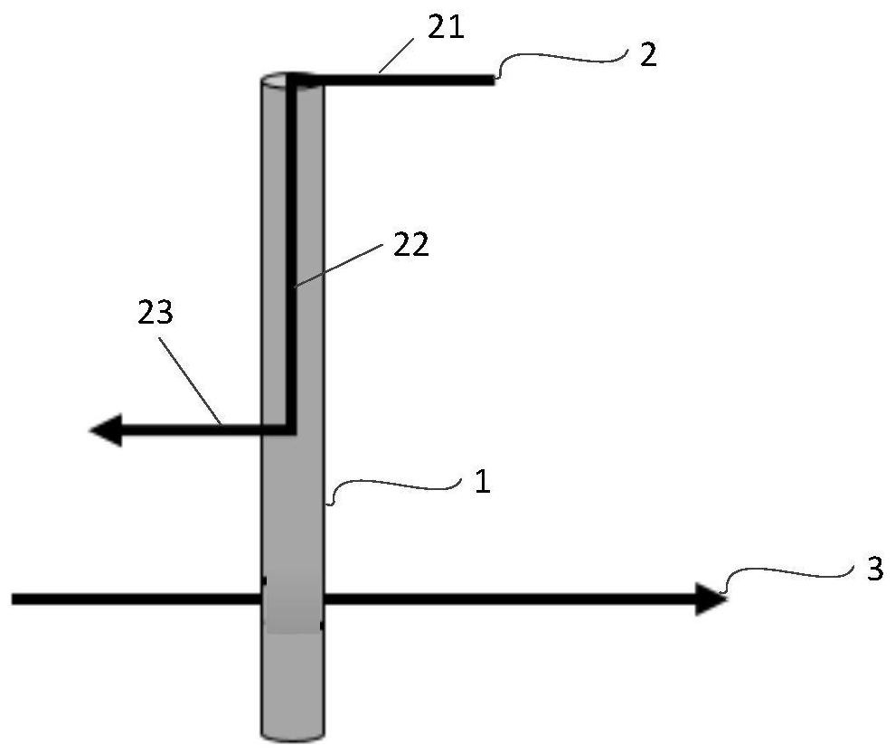
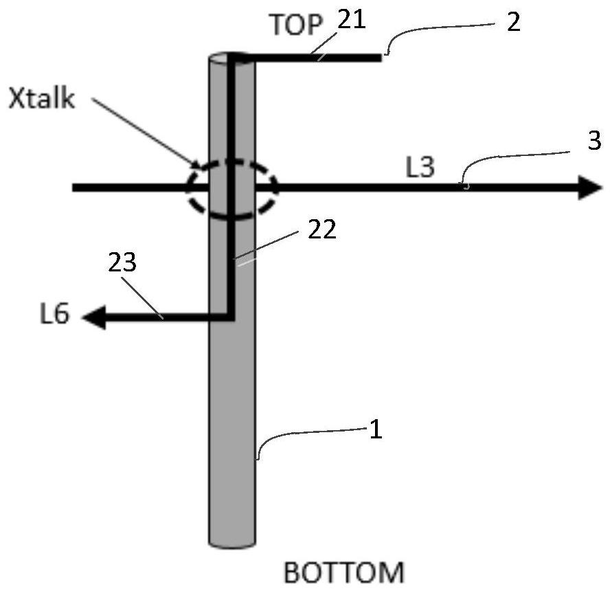
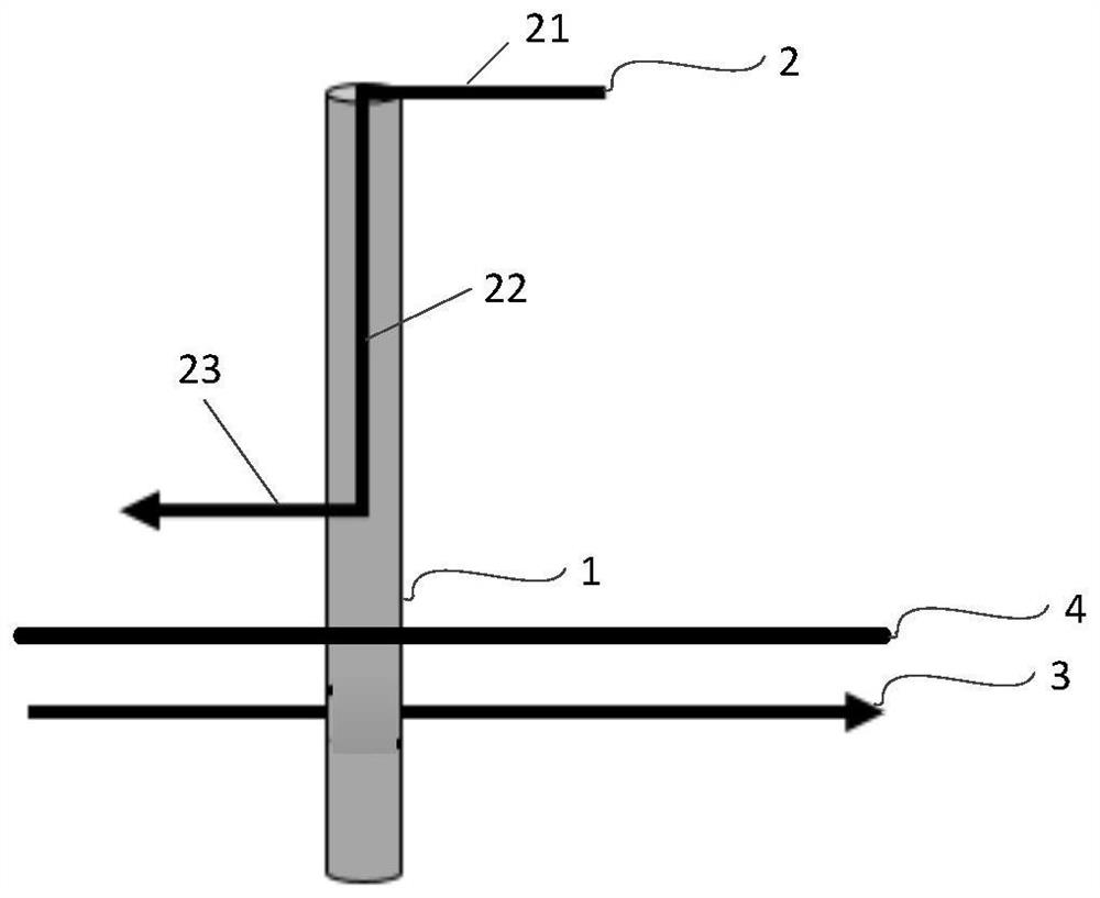
[0028] The embodiment of the present invention provides a PCB board and a method of fabricating a method, and an apparatus capable of reducing the interference between the traces without increasing the trace and the signal via spacing during use, facilitating the implementation of the PCB board. High density design.

[0029] In order to make the objects, technical solutions, and advantages of the present invention more clearly, the technical solutions in the embodiments of the present invention will be described in contemplation in the embodiment of the present invention. It is an embodiment of the invention, not all of the embodiments. Based on the embodiments of the present invention, all other embodiments obtained by those of ordinary skill in the art are in the range of the present invention without making creative labor premise.

[0030] Please refer to figure 1 , figure 1 A schematic structural view of a PCB board provided by the embodiment of the present invention.

[0031]...


PUM


Abstract

The invention discloses a PCB, and a manufacturing method and equipment thereof. The PCB comprises a signal via hole which is formed in the vertical direction, a first wire which passes through the interior of the signal via hole, and a second wire which is arranged in the horizontal direction and is located at the outer side of the signal via hole, wherein a first section of the first wire is located on a first surface layer of the PCB, a second section of the first wire is located inside the signal via hole, a third section of the first wire is located on an inner layer of the PCB, and the second wire is located on the inner layer of the PCB and is not overlapped with the first wire. According to the PCB, the third section of the first wire is located in the inner layer of the PCB, the second wire is further located in the inner layer of the PCB, the second wire and the first wire do not overlap, interference between the second wire and the first wire is reduced under the condition that the distance between the second wire and the signal via hole is not increased, and high-density design of the PCB is achieved.

Description

technical field [0001] The invention relates to the technical field of printed circuits, in particular to a PCB board and a manufacturing method and equipment thereof. Background technique [0002] With the increasing integration of chips, the current society has higher and higher requirements for the miniaturization and high density of electronic products. In order to achieve enough functions in a limited space, it is inevitable that there will be interference between power vias and signal traces due to layout restrictions. In order to reduce interference, it is necessary to maintain sufficient spacing between power vias and traces, which will cause It is more difficult to realize high-density PCB (Printed Circuit Board, printed circuit board) design. At the same time, the Phase / FET and high-voltage vias of the common Buck (step-down) circuit interfere with the surrounding wiring and vias, which often lead to probabilistic problems in the product system. Due to the unconve...

Claims


Application Information

Patent Timeline
IPC IPC(8): H05K1/02H05K3/00
CPCH05K1/02H05K3/00
Inventor 张毅军
Owner SUZHOU LANGCHAO INTELLIGENT TECH CO LTD
Why Eureka
Try Eureka