Monolithic heterogeneous integrated structure and preparation method thereof

A heterogeneous, monolithic technology, used in semiconductor/solid-state device manufacturing, semiconductor devices, electrical components, etc., can solve the problems of Si-based wafer fabrication of devices and circuits, and achieve improved anti-signal crosstalk and anti-radiation. Capability, high-density integrated circuit design, the effect of realizing integrated circuit design

Pending Publication Date: 2022-07-29
INST OF MICROELECTRONICS CHINESE ACAD OF SCI
View PDF0 Cites 0 Cited by
  • Summary
  • Abstract
  • Description
  • Claims
  • Application Information

AI Technical Summary

Problems solved by technology

[0004] The embodiment of the present application solves the technical problem of difficulty in preparing devices and circuits on Si-based wafers in the monolithic heterogeneous integrated structure in the prior art by providing a monolithic heterogeneous integrated structure and a preparation method, and realizes the convenience of semiconductor devices. The technical effect of the preparation

Method used


Image

  • Monolithic heterogeneous integrated structure and preparation method thereof
  • Monolithic heterogeneous integrated structure and preparation method thereof
  • Monolithic heterogeneous integrated structure and preparation method thereof

Examples


Embodiment 1

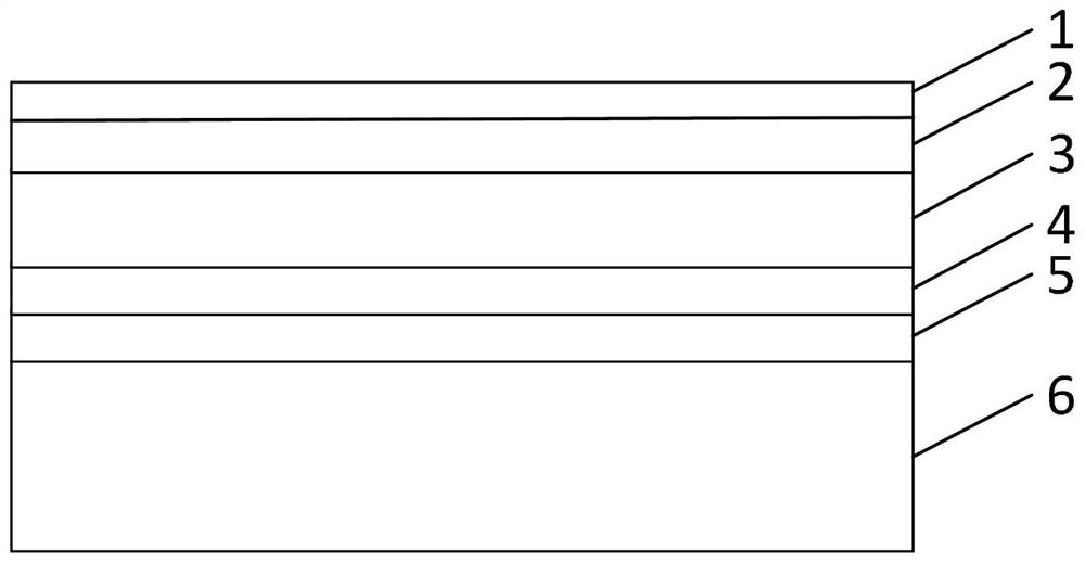
[0055] In this embodiment, a monolithic heterogeneous integrated structure is provided, such as figure 1 shown, including:

[0056] The substrate 6, the nucleation layer 5, the buffer layer 4, the compound semiconductor layer 3, the oxide layer 2 and the silicon layer 1 are sequentially arranged from bottom to top;

[0057] The silicon layer 1 is silicon with a lattice of 100 faces, so that devices and circuits can be fabricated on the silicon layer.

[0058] In an alternative embodiment, the nucleation layer includes at least one of GaN, AlGaN, and AlN, and the buffer layer is GaN, so as to grow the compound semiconductor layer. The compound semiconductor layer is GaN, which has properties such as wide direct band gap, strong atomic bond, high thermal conductivity, good chemical stability, and strong anti-irradiation ability, and can prepare optoelectronic devices, high-temperature and high-power devices and high frequency microwave devices. Of course, the compound semicon...


PUM

PropertyMeasurementUnit
thicknessaaaaaaaaaa
thicknessaaaaaaaaaa

Abstract

The invention discloses a monolithic heterogeneous integrated structure and a preparation method thereof, and the structure comprises a substrate, a nucleating layer, a buffer layer, a compound semiconductor layer, an oxide layer and a silicon layer which are sequentially arranged from bottom to top. The silicon layer is silicon of which the crystal lattice is 100 surfaces, so that a device and a circuit can be conveniently prepared on the silicon layer. And the oxide layer is arranged between the silicon layer and the compound layer, so that the signal crosstalk resistance and the radiation resistance can be improved. Therefore, the technical problem that devices and circuits are difficult to prepare in the Si-based wafer in a monolithic heterogeneous integrated structure in the prior art is solved, and the technical effect of facilitating preparation of semiconductor devices is achieved.

Description

technical field [0001] The invention relates to the field of semiconductors, in particular to a monolithic heterogenous integrated structure and a preparation method. Background technique [0002] Heterogeneous integration can make full use of the special energy band structures and physical properties of different semiconductor materials and other functional materials, not only to manufacture microelectronics and optoelectronic devices with better performance, but also to achieve single-chip integration of discrete devices, promoting electronic systems to small development in the direction of integration and integration. Among them, Si-based compound semiconductors (such as GaN, GaAs and SiC, etc.) have extremely high application prospects in the field of heterogeneous integration technology, such as silicon-based optoelectronics, smart power devices and integrated circuits. Due to high application requirements, silicon-based heterogeneous integration is considered as a tec...

Claims


Application Information

Patent Timeline
Patent Type & Authority Applications(China)
IPC IPC(8): H01L27/12H01L21/762
CPCH01L27/1203H01L21/76251H01L21/76254
Inventor 王磊单小婷李博张学文高见头韩郑生滕瑞刘海南赵发展
Owner INST OF MICROELECTRONICS CHINESE ACAD OF SCI
Why Eureka
Try Eureka