
Method for screening MOS (Metal Oxide Semiconductor) device with electric leakage path

A MOS device and path technology, applied in the field of screening MOS devices with leakage paths, can solve problems such as affecting the electrical characteristics of the device, and achieve the effect of solving time-consuming and easy-to-occur omissions, avoiding unfavorable factors, and ensuring reliability and consistency.

Pending Publication Date: 2021-11-30
SEMITRONIX
View PDF5 Cites 0 Cited by
  • Summary
  • Abstract
  • Description
  • Claims
  • Application Information

AI Technical Summary

Problems solved by technology

The common problem is: a test structure corresponds to only the gate (gate) of a specific target device with signal access, and other MOS devices are floating gate (floating gate), because the voltage on the floating gate is not fixed , there is a possibility of opening to a certain extent, which will increase the leakage path (leakage path) of the S / D terminal (source / drain terminal) of the target device, and the corresponding Ioff (off-state current) current value will be too large, so that Analysis that affects the real electrical characteristics of the device
However, for MOS devices at present, there is generally no special attention to the existence of such a leakage path, that is to say, the influence of such a leakage path on the accurate measurement of the electrical characteristics of MOS devices has not been noticed.
Correspondingly, there is no effective method to screen the leakage path

Method used


Image

  • Method for screening MOS (Metal Oxide Semiconductor) device with electric leakage path
  • Method for screening MOS (Metal Oxide Semiconductor) device with electric leakage path
  • Method for screening MOS (Metal Oxide Semiconductor) device with electric leakage path

Examples


Embodiment 1

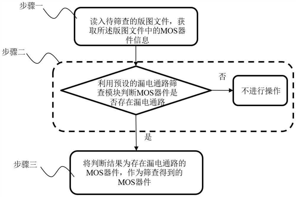
[0025] The method for screening MOS devices with leakage paths in this embodiment, such as figure 1 As shown, it includes: Step 1. Read in the layout file to be screened to obtain the MOS device information in the layout file; Step 2. Use the preset leakage path screening module to determine whether there is a leakage path in the MOS device; Step 3. The judgment result is that the MOS device with a leakage path is used as the screened MOS device. In this embodiment, the preset leakage path screening module defines the conditions for judging whether there is a leakage path in the MOS device. An example of the layout file to be screened is the gds file, and the information of the gds file is obtained to determine whether the source and / or drain of a MOS device is connected to the source and / or drain of other MOS devices. The judgment conditions of the example specifically include: if there is a source terminal and a drain terminal of a certain MOS device connected together with...

Embodiment 2

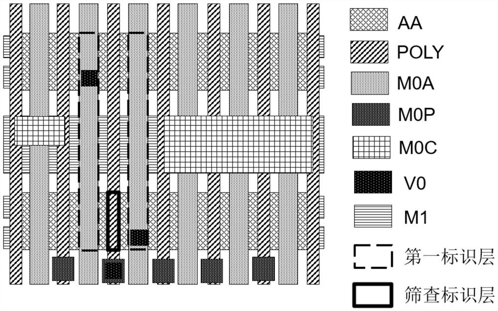
[0028] refer to figure 2In this embodiment, a first identification layer is added to the read-in layout file, and the first identification layer is added with first information for locating the target device; the first information includes: characterizing the source terminal and / or drain terminal of the target device Coordinate information and shape information of the M0 connection line connected to the source terminal and / or drain terminal of other MOS devices (floating gate). The shape information of the M0 connection line is exemplified by its length and width. Wherein, the M0 connection line is in the M0 layer, and is used to connect the active area (AA, ie source or drain) or gate of the MOS device. In this embodiment, the exemplary M0 includes M0A and M0P, M0A is used to connect to the active region (ie source or drain), and M0P is used to connect to the gate. The V0 via is connected to the gate through M0P. In this embodiment, the first identification layer is used ...


PUM


Abstract

The invention provides a method for screening MOS (Metal Oxide Semiconductor) devices with electric leakage paths. The method comprises the following steps of: reading a layout file to be screened, and acquiring MOS device information in the layout file; judging whether the MOS device has an electric leakage path or not by using a preset electric leakage path screening module; and taking the MOS device with the electric leakage path as the MOS device obtained by screening. The steps are simple, the analysis efficiency of the real electrical characteristics of the device is improved, and the reliability of a screening result is high. The technology research and development cost can be reduced, the problems that manual inspection is time-consuming and careless omissions are easy to generate are solved, and when the number of MOS devices is large, the advantage of using the electric leakage path screening module to carry out automatic screening is particularly obvious; and adverse factors existing in analysis of the real electrical characteristics of the device are avoided.

Description

technical field [0001] The invention belongs to the technical field of semiconductor design and manufacture, and in particular relates to a method for screening MOS devices with leakage paths. Background technique [0002] In the semiconductor industry, whether the chip can work normally is of great concern. From the perspective of circuit composition, the chip is composed of devices, and the electrical characteristics of the device itself are crucial to the entire chip. The electrical characteristics of the device can be preliminarily obtained through simulation, which is simulation (Simulation) data; after the chip is produced, the test (Silicon) data is obtained by measuring the device. Compare simulated data with test data (S2S). By comparison, verify the accuracy of the simulation data and assist in judging the correctness of the test data. If the simulation data can accurately reflect the real electrical characteristics of the device, it can be used to design new dev...

Claims


Application Information

Patent Timeline
Patent Type & Authority Applications(China)
IPC IPC(8): H01L21/66H01L23/544
CPCH01L22/34H01L22/32H01L22/20
Inventor 王莹雪方益
Owner SEMITRONIX
Learn More