Chip bonding pad structure, chip, wafer and chip bonding pad structure manufacturing method
A chip pad and manufacturing method technology, applied in semiconductor/solid-state device manufacturing, semiconductor/solid-state device components, semiconductor devices, etc., can solve problems such as chip function failure, avoid virtual soldering, ensure effective contact, and improve reliability. sexual effect
- Summary
- Abstract
- Description
- Claims
- Application Information
AI Technical Summary
Problems solved by technology
Method used
Image

Examples
Embodiment 1
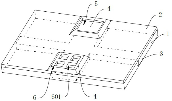
[0062] figure 1 It is a schematic diagram of the chip pad structure provided by an embodiment of the present invention, such as figure 1 As shown, the chip pad structure includes:
[0063] The first insulating layer 1 has grooves;
[0064] The first metal layer 3 is filled in the groove of the first insulating layer 1, and the first metal layer 3 is connected with the internal circuit of the chip to form a conductive channel;
[0065] The second metal layer 4 is formed on the first metal layer 3, and the second metal layer 4 has a pad area for connecting the chip to an external device;
[0066] The second insulating layer 2 covers at least the part of the second metal layer 4 outside the pad area and the first metal layer 3;
[0067] The pad area includes a test pad area 5 and a gold bump pad area 6; the gold bump pad area 6 includes a plurality of sub-pad areas. Among them, the test pad area 5 is used for connecting pads for CP testing after the chip is manufactured, and ...
Embodiment 2
[0101] image 3 It is a schematic diagram of the chip pad structure provided by another embodiment of the present invention, such as image 3 As shown, the chip pad structure includes:
[0102] The first insulating layer 1 has grooves;
[0103] The first metal layer 3 is filled in the groove of the first insulating layer 1, and the first metal layer 3 is connected with the internal circuit of the chip to form a conductive channel;
[0104] The second metal layer 4 is formed on the first metal layer 3, and the second metal layer 4 has a pad area for connecting the chip to an external device;
[0105] The second insulating layer 2 covers at least the part of the second metal layer 4 outside the pad area and the first metal layer 3;
[0106] The pad area includes a test pad area 5 and a gold bump pad area 6; the gold bump pad area 6 includes a plurality of sub-pad areas. Among them, the test pad area 5 is used for connecting pads for CP testing after the chip is manufactured,...
Embodiment 3
[0140] Figure 5 It is a schematic diagram of the chip pad structure provided by another embodiment of the present invention, such as image 3 As shown, the chip pad structure includes:
[0141] The first insulating layer 1 has grooves;
[0142] The first metal layer 3 is filled in the groove of the first insulating layer 1, and the first metal layer 3 is connected with the internal circuit of the chip to form a conductive channel;
[0143] The second metal layer 4 is formed on the first metal layer 3, and the second metal layer 4 has a pad area for connecting the chip to an external device;
[0144] The second insulating layer 2 covers at least the part of the second metal layer 4 outside the pad area and the first metal layer 3;
[0145] The pad area includes a test pad area 5 and a gold bump pad area 6; the gold bump pad area 6 includes a plurality of sub-pad areas. Among them, the test pad area 5 is used for connecting pads for CP testing after the chip is manufactured...
PUM
 Abstract
Description
Claims
Application Information
 - R&D
- Intellectual Property
- Life Sciences
- Materials
- Tech Scout
- Unparalleled Data Quality
- Higher Quality Content
- 60% Fewer Hallucinations
Browse by: Latest US Patents, China's latest patents, Technical Efficacy Thesaurus, Application Domain, Technology Topic, Popular Technical Reports.
© 2025 PatSnap. All rights reserved.Legal|Privacy policy|Modern Slavery Act Transparency Statement|Sitemap|About US| Contact US: help@patsnap.com