
Synchronous carrier modulation method and device for three-level inverter

A three-level inverter and carrier modulation technology, which is applied in the direction of output power conversion device, electrical components, AC power input conversion to DC power output, etc., can solve the problem of optimizing output voltage harmonic performance and common mode voltage performance, Combining problems such as research and cumbersome steps to achieve the effect of optimizing output voltage harmonic performance, optimizing common mode voltage performance, and simple calculation

Pending Publication Date: 2021-12-07
SHENZHEN INVT ELECTRIC
View PDF0 Cites 1 Cited by
  • Summary
  • Abstract
  • Description
  • Claims
  • Application Information

AI Technical Summary

Problems solved by technology

[0010] The above studies only focus on the synchronous modulation or the suppression of common-mode voltage modulation of the three-level inverter, but do not combine the two, and fail to optimize the output voltage harmonic performance and common-mode voltage performance at the same time.
In addition, the above modulation methods are all realized based on space vector synthetic reference voltage, and all need to calculate the action time of each space vector and preset the switching action mode in each space angle area. The steps are cumbersome and the calculation is complicated, which is not conducive to engineering popularization and application.

Method used


Image

  • Synchronous carrier modulation method and device for three-level inverter
  • Synchronous carrier modulation method and device for three-level inverter
  • Synchronous carrier modulation method and device for three-level inverter

Examples


Embodiment Construction

[0082] The following will clearly and completely describe the technical solutions in the embodiments of the present invention with reference to the accompanying drawings in the embodiments of the present invention. Obviously, the described embodiments are only some, not all, embodiments of the present invention. Based on the embodiments of the present invention, all other embodiments obtained by persons of ordinary skill in the art without making creative efforts belong to the protection scope of the present invention.

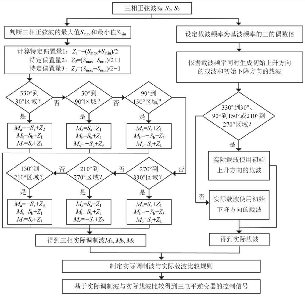
[0083] For the three-level inverter, the present invention obtains three sets of three-phase initial modulation waves by inverting the three-phase sine waves and injecting preset offsets respectively; Corresponding to the three-phase initial modulation wave, the three-phase actual modulation wave is obtained; the carrier frequency is obtained according to the carrier wave in the first preset direction and the second preset direction to obtain the first carrier ...


PUM


Abstract

The invention discloses a synchronous carrier modulation method for a three-level inverter, and the method comprises the steps: carrying out the negation of a three-phase sine wave, and injecting a specific offset, and obtaining three groups of three-phase initial modulation waves; respectively selecting specific initial modulation waves for three phases in different space angle regions to obtain three-phase actual modulation waves; obtaining two groups of carriers with opposite initial directions by setting the triangular carrier frequency to be the even number times of three of the fundamental wave frequency; selecting specific initial direction carriers in different space angle areas to obtain actual carriers; and formulating a comparison rule of the actual modulation wave and the actual carrier wave, and obtaining a control signal of the three-level inverter based on comparison of the actual modulation wave and the actual carrier wave, thereby realizing synchronous carrier wave modulation for reducing the common-mode voltage. According to the method, the amplitude of the common-mode voltage can be reduced by one half while harmonic waves of multiple of three and even harmonic waves in the line voltage are eliminated, the change frequency of the common-mode voltage can be reduced by two thirds, and the method has the advantages of being simple in calculation and convenient to implement.

Description

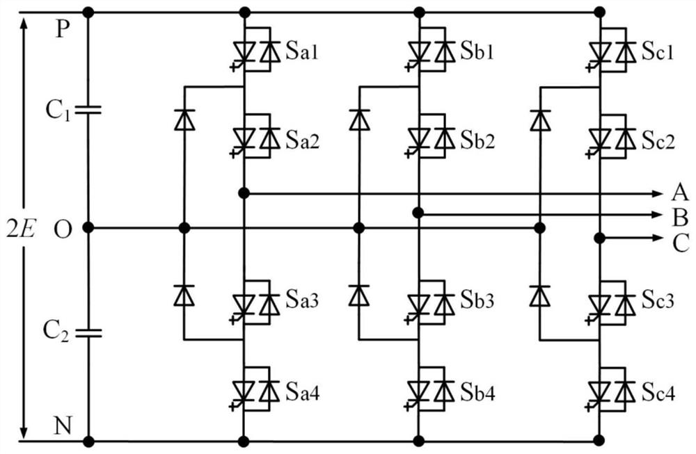
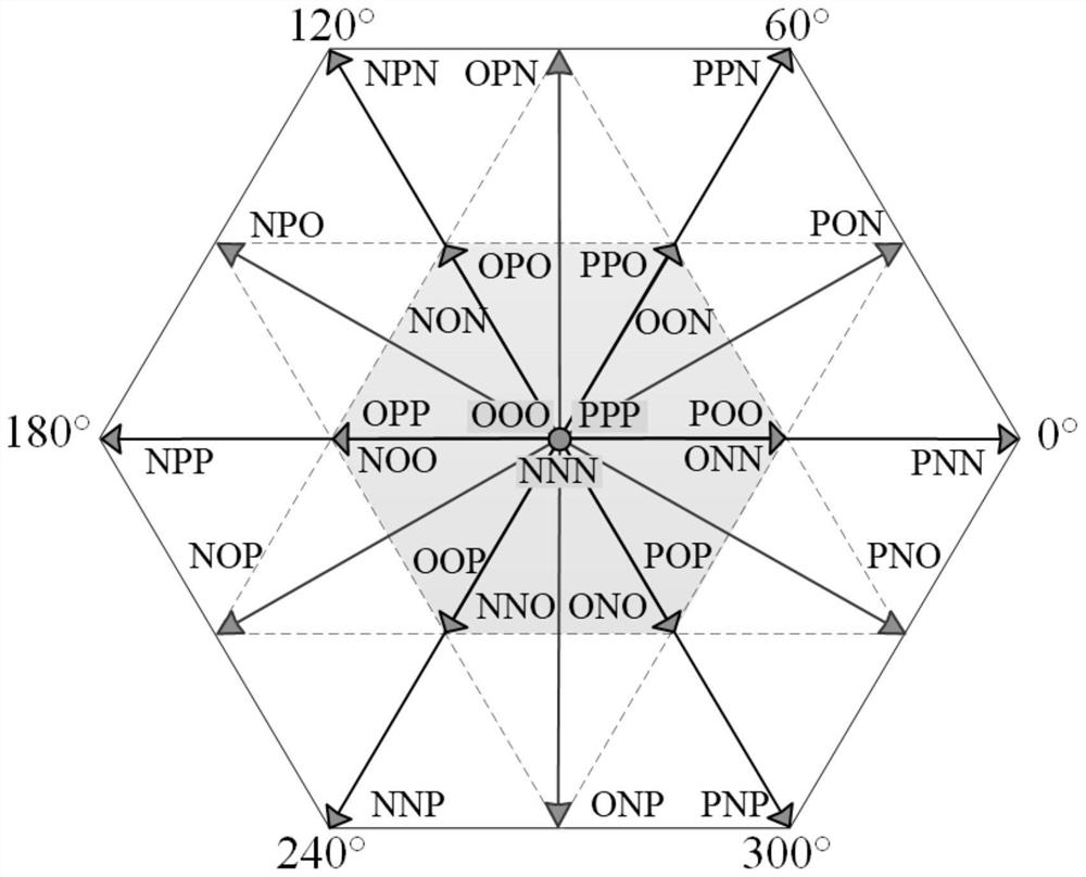
technical field [0001] The invention relates to a PWM control method, in particular to a three-level inverter synchronous carrier modulation method and device. Background technique [0002] A typical three-level inverter such as a three-level neutral point clamped (Neutral Point Clamped, NPC) inverter, its main circuit topology is as follows figure 1 . Due to the advantages of low device voltage stress, high output voltage and current quality, simple structure, and bidirectional flow of energy, three-level inverters have been widely used in fields such as motor drive, new energy power generation, and mining shields. [0003] Define the three level states of the three-level inverter output from high to low as P, O and N, and the DC side voltage is 2E, then the space vector of the three-level inverter can be summarized in figure 2 . figure 2 Each space vector in can be classified into zero vector, small vector, medium vector and large vector according to the magnitude. Th...

Claims


Application Information

Patent Timeline
Patent Type & Authority Applications(China)
IPC IPC(8): H02M7/487H02M7/501H02M7/5387H02M7/5395H02M1/12
CPCH02M7/487H02M7/501H02M7/53875H02M7/5395H02M1/12
Inventor 高瞻周志达耿程飞赖娜谢扬旭王宇宋茂林吴轩钦
Owner SHENZHEN INVT ELECTRIC
Learn More