
Wafer cleaning device

A technology for cleaning devices and wafers, applied in cleaning methods and utensils, cleaning methods using tools, cleaning methods using liquids, etc., can solve problems such as slow soaking of cleaning liquids, long cleaning time, and reduced cleaning efficiency, etc. Achieve the effect of fast infiltration speed, shortened cleaning time and high cleaning efficiency

Pending Publication Date: 2021-12-10
WUHAN UNIV OF TECH
View PDF1 Cites 1 Cited by
  • Summary
  • Abstract
  • Description
  • Claims
  • Application Information

AI Technical Summary

Problems solved by technology

[0005] In view of this, it is necessary to provide a wafer cleaning device to solve the problem that in the existing cleaning device, the speed at which the cleaning brush infiltrates the cleaning liquid is slow, the cleaning liquid sprayed onto the wafer is lost quickly, and the cleaning time is relatively time-consuming. Long, the problem of reducing cleaning efficiency

Method used


Image

  • Wafer cleaning device
  • Wafer cleaning device
  • Wafer cleaning device

Examples


Embodiment Construction

[0021] Preferred embodiments of the present invention will be described in detail below in conjunction with the accompanying drawings, wherein the accompanying drawings constitute a part of the application and together with the embodiments of the present invention are used to explain the principle of the present invention and are not intended to limit the scope of the present invention.

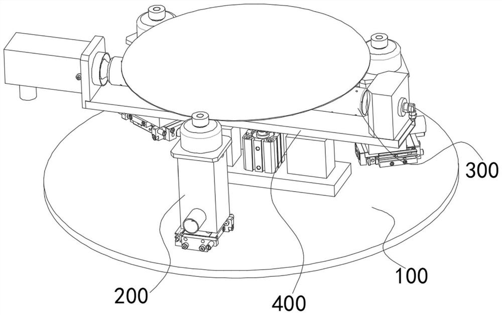
[0022] like figure 1 As shown, a wafer cleaning device in this embodiment is used to clean wafers, including a workbench 100, a rotary clamping assembly 200 and a cleaning assembly 300, wherein the rotary clamping assembly 200 is arranged on the workbench 100 and rotates The clamping assembly 200 is used to clamp the wafer and drive the wafer to rotate. The cleaning assembly 300 is attached to the wafer, and the wafer is cleaned by soaking the cleaning assembly 300. The cleaning speed is faster. More detailed explanation and illustrate.

[0023] The wafer in this embodiment is set on the wor...


PUM


Abstract

The invention relates to a wafer cleaning device which is used for cleaning a wafer and comprises a workbench, a rotary clamping assembly and a cleaning assembly. The wafer is arranged on the workbench. The rotary clamping assembly is arranged on the workbench, the rotary clamping assembly is provided with at least three rotary ends, the at least three rotary ends are evenly arranged in the circumferential direction of the wafer, the rotary directions of the at least three rotary ends are the same, and the at least three rotary ends abut against the thin edge of the wafer and are used for driving the wafer to rotate in the axis direction of the wafer. The cleaning assembly comprises a horizontally-arranged cleaning brush, the cleaning brush is rotatably connected with the workbench, the cleaning brush is attached to the surface of the wafer, a cavity is formed in the cleaning brush, the cavity is communicated with the outer surface of the cleaning brush, the cleaning brush enables the cavity to be externally connected with a cleaning medium through a rotary joint, and the wafer can be cleaned through rotation of the wetted cleaning brush. The problems that in an existing cleaning device, the speed of soaking a cleaning brush in a cleaning solution is low, the loss speed of the cleaning solution sprayed onto the wafer is high, the cleaning time is long, and the cleaning efficiency is lowered are solved.

Description

technical field [0001] The invention relates to the technical field of semiconductor material processing, in particular to a wafer cleaning device. Background technique [0002] With the rapid development of semiconductor manufacturing technology, CMP (Chemical Mechanical Polishing) has become a key technology for realizing multi-metal layers and interconnection lines in wafer manufacturing. performance of subsequently formed semiconductor devices. After the wafer is chemically mechanically polished, the surface of the wafer often has residual polishing liquid and foreign matter, so the cleaning of the wafer has become a very important and demanding process. [0003] For example, the wafer cleaning device whose application number is CN202011472545.4 proposes a wafer cleaning device that can dynamically adjust the attitude, by setting a wafer rotation assembly, two cleaning brushes on both sides of the wafer, a cleaning brush movement mechanism and a controller , can effect...

Claims


Application Information

Patent Timeline
IPC IPC(8): B08B1/02B08B3/08B08B13/00H01L21/67H01L21/687
CPCB08B3/08B08B13/00H01L21/67046H01L21/68721H01L21/68764B08B1/12B08B1/20Y02P70/50
Inventor 吴超群张旭焱梁穆熙胡智杰
Owner WUHAN UNIV OF TECH
Features
  • Generate Ideas
  • Intellectual Property
  • Life Sciences
  • Materials
  • Tech Scout
  • Unparalleled Data Quality
  • Higher Quality Content
  • 60% Fewer Hallucinations
Learn More