
Chip frame fixing support of semiconductor chip wire bonding equipment

A technology for fixing brackets and semiconductors, which is applied in semiconductor/solid-state device manufacturing, electrical components, circuits, etc. It can solve the problems of frame shaking, offset, unavoidable chip frame warping or vibration, and high defect rate, so as to reduce the number of products The scrap rate and the effect of avoiding bad solder joints

Pending Publication Date: 2021-12-14
SHANTOU HUSN ELECTRONICS DEVICES
View PDF2 Cites 0 Cited by
  • Summary
  • Abstract
  • Description
  • Claims
  • Application Information

AI Technical Summary

Problems solved by technology

However, during the wire welding process, the frame will shake and shift, and there will be problems such as false welding of solder joints, poor solder joints, and failure to press, resulting in a high defect rate in the production process
[0003] CN112108827A discloses a pressing plate device, which includes a pressing plate frame capable of pressing the product to be welded. The pressing plate frame is provided with an operation window capable of exposing the welding area of ​​the product to be welded. The first auxiliary platen assembly located in the operation window to be pressed by the area to be welded solves the problem of high product scrap rate to a certain extent, but because the overall chip frame is uneven rather than a flat plate, the chip frame cannot be avoided during the wire bonding process. Problems with warping or vibration, product scrap rate is still high
However, the problem of chip frame warping or vibration during the wire bonding process cannot be avoided, and the product scrap rate is still high

Method used


Image

  • Chip frame fixing support of semiconductor chip wire bonding equipment
  • Chip frame fixing support of semiconductor chip wire bonding equipment
  • Chip frame fixing support of semiconductor chip wire bonding equipment

Examples


Embodiment Construction

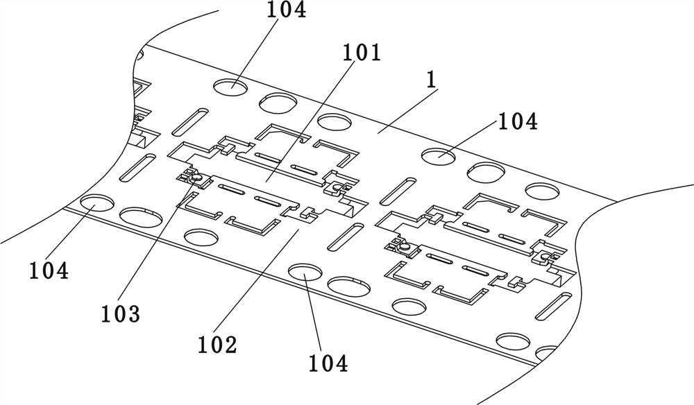
[0029] figure 1 It is a schematic diagram of the structure of the chip frame, which is a chip frame 1 of the TO-270 package type. It is composed of a small bottom plate 101 and a large upper plate 102. The connecting column 103 at the end is connected with the connecting piece formed by the downward bending of the upper plate 102 . There are two steps formed by a bottom plate 101 and an upper flat plate 102 on its side. After wire bonding, the semiconductor chip is fixed on the base plate 101 and connected with wires. When ultrasonic bonding wires are used, in order to avoid defective solder joints caused by warping of the chip frame caused by ultrasonic vibration, it is necessary to fix each part of the chip frame 1 respectively.

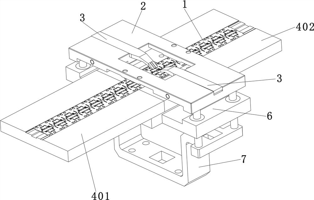
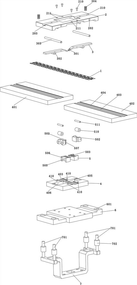
[0030] Figure 2-Figure 8 Showing an embodiment of the present invention, the chip frame fixing bracket includes a platen pressing mechanism, a central track module, a chip frame positioning mechanism, a retractable insertion piece, and a drivin...


PUM


Abstract

The invention discloses a chip frame fixing support of semiconductor chip wire bonding equipment, and the support comprises a pressing plate mechanism which is provided with a liftable pressing plate and an elastic pressing claw installed on the pressing plate, wherein the elastic pressing claw tightly presses a chip frame when the pressing plate descends; a central rail module, wherein the upper part of the central rail module is provided with a rail for the sliding of the chip frame, and the side part of the rail is provided with a concave step for the insertion of the telescopic insertion sheet; telescopic insertion pieces which are located on the two sides of the center rail, wherein the insertion pieces are driven to clamp the chip frame from the side direction when the pressing plate descends; a plurality of positioning pins which are used for jointing and positioning the pressing plate, the chip frame and the central track when the pressing plate descends; and a driving mechanism which is connected with the power source and the pressing plate and can drive the pressing plate to ascend and descend and can fix all parts of the chip frame, so that the problems of poor welding spots and the like caused by vibration of the chip frame in the wire welding process are solved.

Description

technical field [0001] The invention relates to semiconductor chip packaging equipment, in particular to a chip frame fixing bracket used in semiconductor chip wire bonding equipment. Background technique [0002] The wire bonding process is a key production link in the semiconductor packaging process. In the process of wire bonding, it is necessary to use wires to weld the chip and frame pins together, use ultrasonic waves or heating blocks for wire bonding, use a pressure plate to press and fix the frame, and then perform wire bonding. However, during the wire welding process, the frame will shake and shift, and there will be problems such as false welding of solder joints, poor solder joints, and failure to press, resulting in a high defect rate in the production process. [0003] CN112108827A discloses a pressing plate device, which includes a pressing plate frame capable of pressing the product to be welded. The pressing plate frame is provided with an operation window...

Claims


Application Information

Patent Timeline
IPC IPC(8): H01L21/687H01L21/68
CPCH01L21/68728H01L21/68742H01L21/68785H01L21/68
Inventor 李彬林广平杨燮斌方逸裕
Owner SHANTOU HUSN ELECTRONICS DEVICES
Learn More