Device and method for improving process deviation of multi-cavity equipment

A process deviation, multi-chamber technology, used in the manufacture of discharge tubes, electrical components, semiconductor/solid-state devices, etc., can solve the problems of film thickness difference on the wafer surface, increase the structure of the gas supply system, and affect the wafer yield. , to achieve the effect of reducing film thickness difference, efficient gas channeling, and improving wafer yield

Pending Publication Date: 2021-12-21
PIOTECH CO LTD
View PDF0 Cites 0 Cited by
  • Summary
  • Abstract
  • Description
  • Claims
  • Application Information

AI Technical Summary

Problems solved by technology

[0002] In the field of semiconductor manufacturing, a variety of gases are widely used to react on the surface of the wafer to complete coating or etching processes. At this stage, in order to increase production capacity and reduce costs, when processing and cleaning chambers, multiple chambers often share a group of reactions In this way, a circuit structure of interconnection between chambers is formed, that is, under the process state, considering the difference in flow resistance between chambers, the reaction gas will also flow through the circuit of the cleaning chamber when it flows to its own chamber to other chambers, which causes differences in the thickness of the film on the wafer surface between the chambers, which affects the yield of the wafer
[0003] In response to this problem, at this stage, some adopt the isolation valve scheme, and some adopt the independent gas supply scheme between the chambers to prevent the gas from flowing to other chambers. Regarding the technical scheme of the isolation valve, the isolation valve will produce particles after a long period of use The problem is that for the independent gas supply scheme, the structure of the gas supply system will inevitably be enlarged, which will make the machine too compact and complicated, and at the same time greatly increase the cost of the machine

Method used


Image

  • Device and method for improving process deviation of multi-cavity equipment
  • Device and method for improving process deviation of multi-cavity equipment
  • Device and method for improving process deviation of multi-cavity equipment

Examples


Embodiment Construction

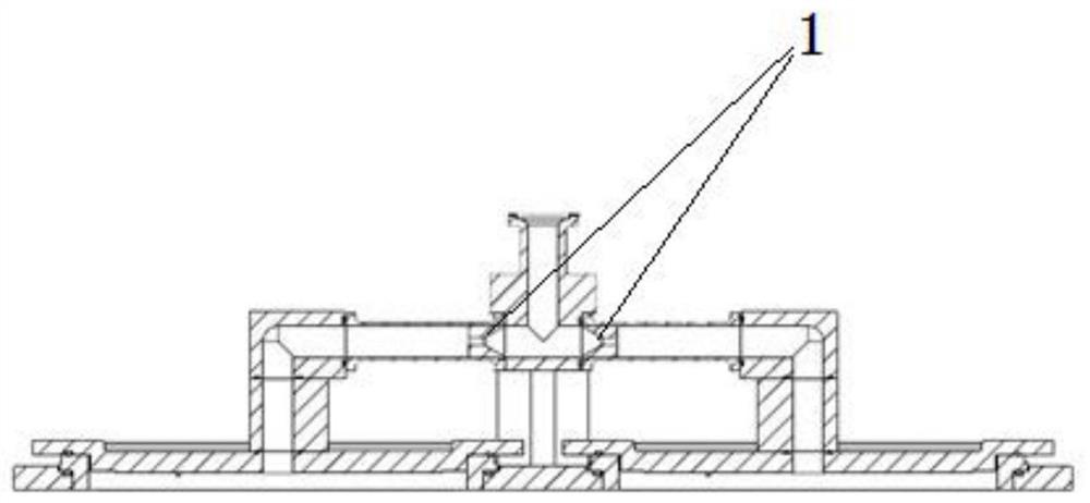
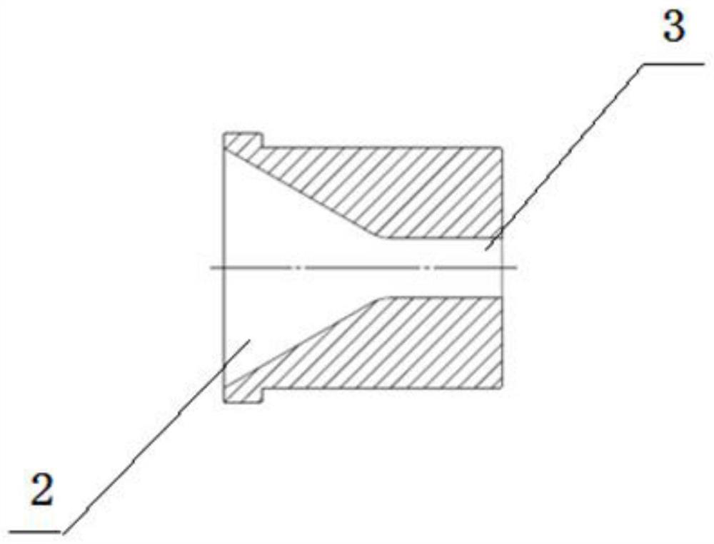
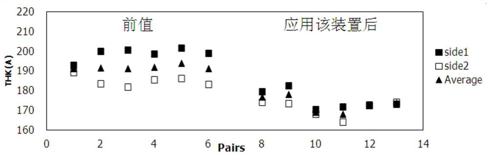
[0021] Such as figure 1 As shown, it is a schematic diagram of the installation position of the device. This embodiment aims at the problem of the difference in film thickness of the wafer surface between the chambers caused by the channeling of the process gas between the chambers in the prior art, and provides a method for reducing the thickness of the film between the chambers. The thickness difference device 1 mainly includes positioning steps, a tapered surface structure 2, and a straight hole structure 3; through this device, the difference in film thickness on the wafer surface between chambers is reduced, and the yield of wafers is improved.

[0022] The positioning step positions the device on the air path;

[0023] For further improvement, the thickness of the step meets the tolerance requirement of 0, -0.02. Reasonable tolerance requirements, on the one hand, prevent the O-ring seals on other gas paths from being compressed and fail to cause gas leakage due to ther...


PUM

PropertyMeasurementUnit
thicknessaaaaaaaaaa

Abstract

The invention provides a device and method for improving process deviation of multi-chamber equipment. The device is arranged on a multi-chamber reaction gas path, one end of the interior of the device adopts a conical surface structure, and the other end of the interior of the device adopts a straight hole structure. According to the device and the method provided by the invention, the structure/operation is simple, the price is low, the problem of high-efficiency blocking of gas channeling can be achieved by reasonably setting the internal aperture, finally, the thickness difference of the wafer surface film between the chambers is reduced, and the yield of the wafer is improved.

Description

technical field [0001] The invention belongs to the technical field of semiconductor manufacturing, and relates to a device and a method for improving the process deviation of multi-chamber equipment. Background technique [0002] In the field of semiconductor manufacturing, a variety of gases are widely used to react on the surface of the wafer to complete coating or etching processes. At this stage, in order to increase production capacity and reduce costs, when processing and cleaning chambers, multiple chambers often share a group of reactions In this way, a circuit structure of interconnection between chambers is formed, that is, under the process state, considering the difference in flow resistance between chambers, the reaction gas will also flow through the circuit of the cleaning chamber when it flows to its own chamber To other chambers, this will cause differences in the thickness of the film on the surface of the wafer between the chambers, which will affect the ...

Claims


Application Information

Patent Timeline
Patent Type & Authority Applications(China)
IPC IPC(8): H01J37/32H01L21/67
CPCH01J37/32798H01L21/67155
Inventor 周仁侯彬荒见淳一柴智安超
Owner PIOTECH CO LTD
Why Eureka
Try Eureka