Supercharge Your Innovation With Domain-Expert AI Agents!

Semiconductor structure and forming method thereof

A semiconductor and sidewall technology, applied in the field of semiconductor structures and their formation, can solve problems such as the difficulty of the channel and the deterioration of the gate structure's ability to control the channel, so as to achieve a small leakage current probability, a small on-current, and a low power consumption. low cost effect

Pending Publication Date: 2021-12-24
SEMICON MFG INT (SHANGHAI) CORP +1
View PDF2 Cites 0 Cited by
  • Summary
  • Abstract
  • Description
  • Claims
  • Application Information

AI Technical Summary

Problems solved by technology

However, as the channel length of the device is shortened, the distance between the source and the drain of the device is also shortened, so the ability of the gate structure to control the channel becomes worse, and the gate voltage pinches off the channel. The difficulty of the channel is also increasing, making the phenomenon of subthreshold leakage (subthreshold leakage), the so-called short-channel effect (SCE: short-channel effects) more likely to occur

Method used


Image

  • Semiconductor structure and forming method thereof
  • Semiconductor structure and forming method thereof
  • Semiconductor structure and forming method thereof

Examples


Embodiment Construction

[0013] It can be seen from the background art that the devices formed so far still have the problem of poor performance. The reasons for the poor performance of the device are analyzed in conjunction with a method of forming a semiconductor structure.

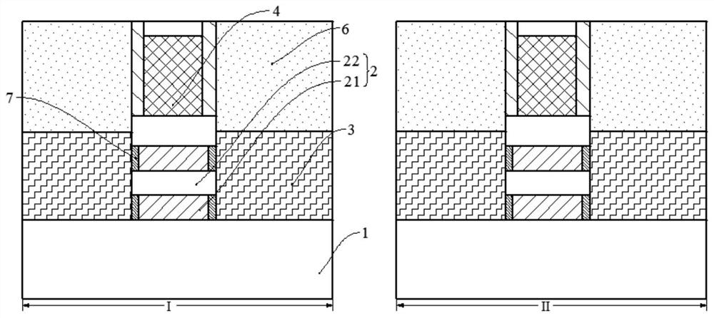
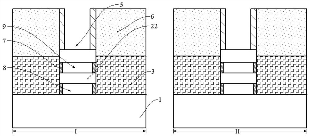
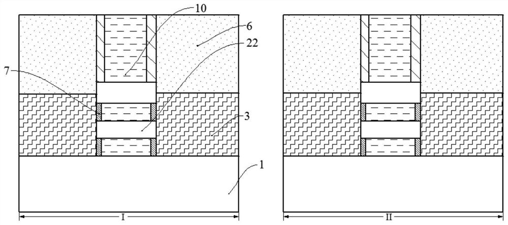
[0014] refer to Figure 1 to Figure 3 , shows a structural schematic diagram of key steps in a method for forming a semiconductor structure.

[0015] Such as figure 1 As shown, the substrate includes a first region I and a second region II, including a substrate 1 and a channel stack 2 on the substrate 1, and the channel stack 2 includes a sacrificial layer 21 and The channel layer 22 located on the sacrificial layer 21; the dummy gate structure 4 located on the channel stack 2, the dummy gate structure 4 covering part of the top wall and part of the sidewall of the channel stack 2 , taking the direction parallel to the surface of the substrate 1 and perpendicular to the extension direction of the dummy gate structure 4 as t...


PUM


Abstract

The invention discloses a semiconductor structure and a forming method thereof. The method comprises the following steps: forming a trench, transversely etching a sacrificial layer exposed out of the trench, forming a first groove, carrying out the transverse etching of the sacrificial layer exposed out of the first groove in a second region, forming a second groove, the transverse size of the sacrificial layer below the gate structure in the second region is smaller than the transverse size of the sacrificial layer below the gate structure in the first region, and after the pseudo gate structure and the sacrificial layer are removed and the gate structure is formed, the transverse size of the contact between the gate structure in the second region and the channel layer is smaller; the lateral dimension of the contact between the gate structure in the first region and the channel layer is large. When the semiconductor structure works, the transverse size of the channel in the first region is larger than that of the channel in the second region, the transistor formed in the first region is small in breakover current, low in power consumption and small in leakage current probability, and the transistor formed in the second region is large in breakover current and high in response speed.

Description

technical field [0001] Embodiments of the present invention relate to the field of semiconductor manufacturing, and in particular, to a semiconductor structure and a method for forming the same. Background technique [0002] In semiconductor manufacturing, with the development trend of ultra-large-scale integrated circuits, the feature size of integrated circuits continues to decrease. In order to adapt to smaller feature sizes, metal-oxide-semiconductor field-effect transistors (Metal-Oxide-Semiconductor Field-Effect Transistor, The channel length of MOSFET) is also continuously shortened accordingly. However, as the channel length of the device is shortened, the distance between the source and the drain of the device is also shortened, so the ability of the gate structure to control the channel becomes worse, and the gate voltage pinches off the channel. The channel becomes more and more difficult, making subthreshold leakage (subthreshold leakage), the so-called short-ch...

Claims


Application Information

Patent Timeline
IPC IPC(8): H01L21/8234H01L21/8238H01L27/088H01L27/092
CPCH01L21/823412H01L21/823431H01L21/823437H01L21/823807H01L21/823821H01L21/823828H01L27/0886H01L27/0924
Inventor 王楠
Owner SEMICON MFG INT (SHANGHAI) CORP
Features
  • R&D
  • Intellectual Property
  • Life Sciences
  • Materials
  • Tech Scout
  • Unparalleled Data Quality
  • Higher Quality Content
  • 60% Fewer Hallucinations
Learn More