Optical device coupling method and system, transmitting optical device and optical module adjusting and testing method

An optical device, a technology for emitting light, applied in the field of optical communication, can solve the problems of yield loss, low product efficiency, multiple human resources, etc., to avoid defective products, reduce product man-hours, and improve commissioning efficiency.

Pending Publication Date: 2022-01-04
WUHAN HUAGONG GENUINE OPTICS TECH
View PDF3 Cites 0 Cited by
  • Summary
  • Abstract
  • Description
  • Claims
  • Application Information

AI Technical Summary

Problems solved by technology

In the actual application process, the optical device performs optical power coupling under the condition of fixed DC, and the actual module parameters OMA / ER / Vbias operating point / Ibias are obtained through AC commissioning, which makes the device coupling condition In this case, the module side needs to continuously perform joint modulation between these parameters. In extreme cases, the module side cannot meet the performance requirements.
In the mass production process, this results in low product efficiency, requires more human resources to maintain or causes a large yield loss

Method used


Image

  • Optical device coupling method and system, transmitting optical device and optical module adjusting and testing method
  • Optical device coupling method and system, transmitting optical device and optical module adjusting and testing method
  • Optical device coupling method and system, transmitting optical device and optical module adjusting and testing method

Examples


Embodiment 1

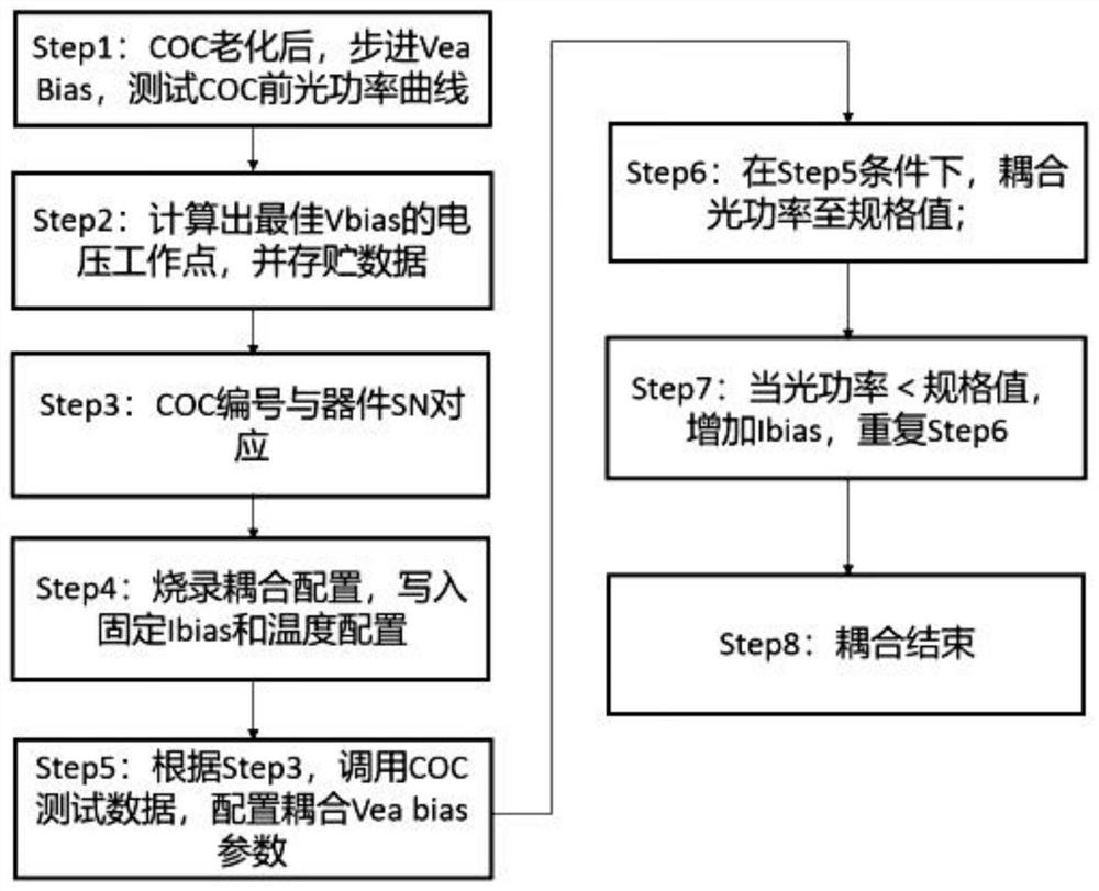
[0040] see figure 1 , the embodiment of the present invention provides a kind of optical device coupling method, is suitable for EML (electroabsorption modulation) laser, comprises the following steps:

[0041] Fix the laser on a specific ceramic substrate to form a COC component;

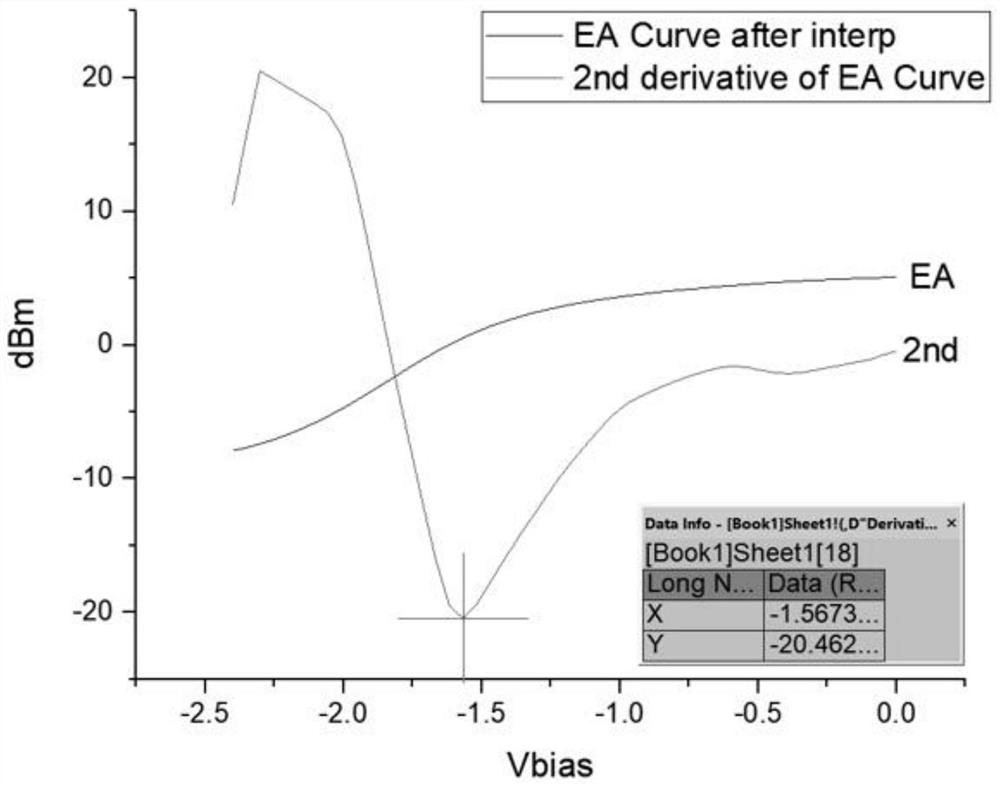
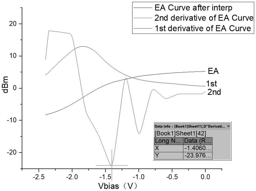
[0042] After the COC component is aged, test the characteristics of its modulation voltage Vbias and its output optical power (hereinafter referred to as the EA absorption characteristic curve) to configure the Vbias bias voltage point during coupling; when testing the EA absorption characteristic curve, the COC component is in a constant and fixed temperature condition Below; when testing the EA absorption characteristic curve, the COC component is under a fixed bias current Ibias;

[0043] Calculate the corresponding optimal Vbias voltage operating point according to the EA absorption characteristic curve of each COC component;

[0044] Assembling the light-emitting device;

[0045] Configure ...

Embodiment 2

[0054] The invention discloses a test module, a data processing module, a storage module, a burning module, a coupling module, an optical power measurement module, and a coupling judgment module;

[0055] The test module is used to test the relationship between the Vbias voltage of the laser and the output optical power curve, that is, the EA absorption characteristic curve;

[0056] The data processing module is used to calculate the corresponding optimal Vbias voltage operating point according to the EA absorption characteristic curve of each laser;

[0057] The storage module is used to save data, including bias current Ibias, temperature, and optimum Vbias voltage value;

[0058] The burning module is used to call the corresponding bias current Ibias, temperature, and optimal Vbias voltage value to be configured in the light-emitting device;

[0059] The coupling module is used to perform optical power coupling on the emitting optical device;

[0060] The optical power m...

Embodiment 3

[0063] This embodiment also discloses an optical emitting device, which is obtained by coupling with the optical device coupling method as described in the first embodiment.


PUM


Abstract

The invention relates to an optical device coupling method, an optical device coupling system, an emitting optical device and an optical module adjusting and testing method. According to the optical device coupling method, the working characteristics of an EA absorption curve of an EML laser are tested, and a voltage working point corresponding to a second-order differential inflection point is calculated through data processing to serve as an optimal Vbias voltage value; then at this operating voltage, the optical power is coupled into the target specification. The working characteristics of the device coupled through the method are very close to the actual working point of the module, and parameters based on the voltage point do not need to be reconfigured or only need to be finely adjusted at the module end. The method has the advantages that the performance risk COC can be recognized in advance, and defective products are prevented from being formed by back-end applications. Meanwhile, module end adjusting and testing efficiency can be greatly improved, and product working hours are reduced.

Description

technical field [0001] The invention belongs to the technical field of optical communication, and in particular relates to an optical device coupling method and system, an optical emitting device and an optical module commissioning method. Background technique [0002] With the popularization of 5G application scenarios, the data center market has higher and higher requirements for transmission capacity. Electroabsorption modulated laser EML has a large bandwidth and modulation rate, and is the mainstream solution for current 400G optical module products. In the actual application process, the optical device performs optical power coupling under the condition of fixed DC, and the actual module parameters OMA / ER / Vbias operating point / Ibias are obtained through AC commissioning, which makes the device coupling condition In this case, the module side needs to continuously perform joint modulation between these parameters, and in extreme cases, the module side cannot meet the p...

Claims


Application Information

Patent Timeline
IPC IPC(8): H04B10/073
CPCH04B10/0731
Inventor 袁新烈迟景茂汤秉凡
Owner WUHAN HUAGONG GENUINE OPTICS TECH
Why Eureka
Try Eureka