Supercharge Your Innovation With Domain-Expert AI Agents!

Method for producing organic EL device

A manufacturing method and technology of EL devices, applied to organic semiconductor devices, electric solid devices, semiconductor devices, etc., can solve problems such as unevenness and inability to reliably form organic barrier layers, and achieve the effect of improving moisture resistance reliability

Pending Publication Date: 2022-01-11
SAKAI DISPLAY PROD
View PDF11 Cites 0 Cited by
  • Summary
  • Abstract
  • Description
  • Claims
  • Application Information

AI Technical Summary

Problems solved by technology

[0011] In this way, the method of forming the organic barrier layer described in Patent Document 1 or 2 only utilizes the surface tension of the liquid resin and does not exist uniformly, so the organic barrier layer may be formed in an unnecessary position.
In addition, conversely, there is also a possibility that the organic barrier layer cannot be reliably formed at the desired position.

Method used


Image

  • Method for producing organic EL device
  • Method for producing organic EL device
  • Method for producing organic EL device

Examples


Embodiment Construction

[0074] Hereinafter, a method of manufacturing an organic EL device according to an embodiment of the present invention and an organic EL device manufactured by such a manufacturing method will be described with reference to the drawings. Hereinafter, an OLED display device is exemplified as an organic EL device. In addition, embodiment of this invention is not limited to embodiment illustrated below.

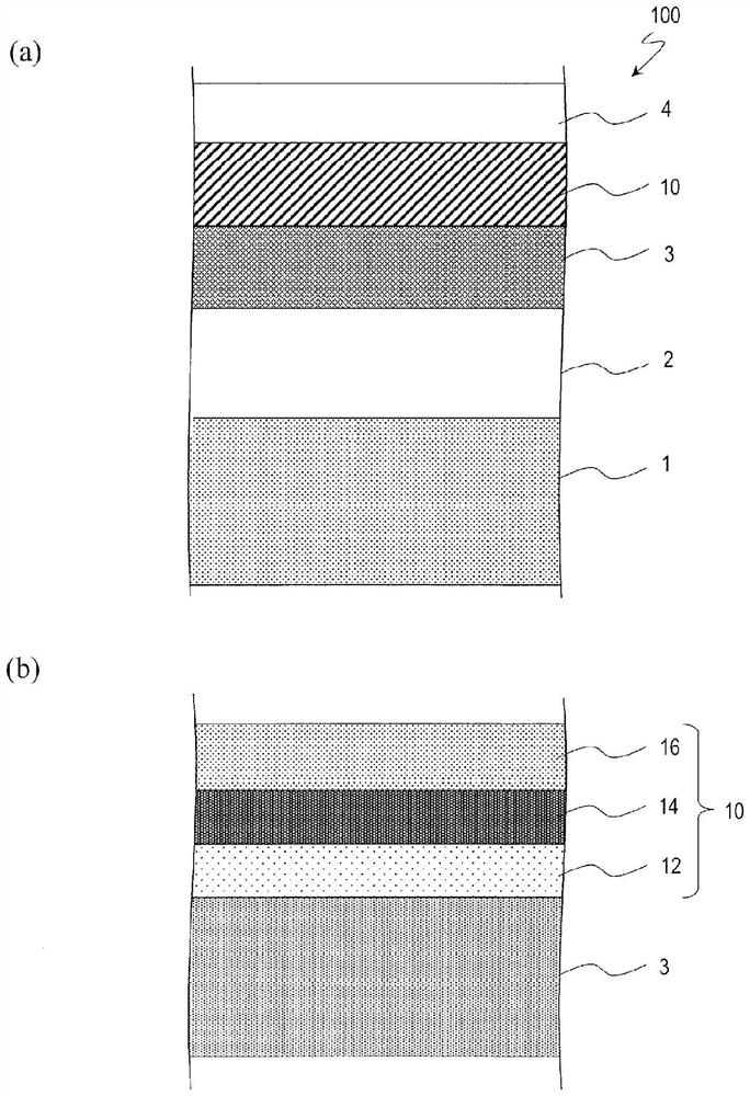
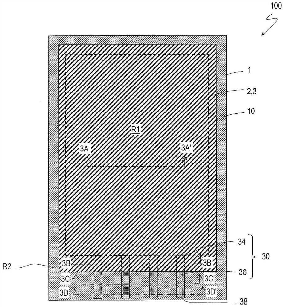
[0075] First, refer to figure 1 (a) and figure 1 (b) illustrates the basic configuration of the OLED display device 100 manufactured by the manufacturing method according to the embodiment of the present invention. figure 1 (a) is a schematic partial cross-sectional view of an active region of an OLED display device 100 according to an embodiment of the present invention, figure 1 (b) is a partial cross-sectional view of the TFE structure 10 formed on the OLED3.

[0076] The OLED display device 100 has a plurality of pixels, and each pixel has at least one organic EL ele...


PUM

PropertyMeasurementUnit
thicknessaaaaaaaaaa
diameteraaaaaaaaaa
volumeaaaaaaaaaa

Abstract

A step for forming a thin film sealing structure (10) in a method for producing an organic EL device comprises: a step A for forming a first inorganic barrier layer (12); a step B for detecting particles having an area equivalent circle diameter of from 0.2 [mu]m to 5 [mu]m (inclusive) below and above the first inorganic barrier layer after the step A, and acquiring location information, size information and shape information of each detected particle and the aspect ratio of each detected particle if the detected particle has an area equivalent circle diameter of 1 [mu]m or more; a step C for applying microdroplets of a coating liquid containing a photocurable resin to each particle by an inkjet method on the basis of the location information; and a step D for irradiating the photocurable resin with ultraviolet light after the step C so as to cure the photocurable resin, thereby forming an organic barrier layer (14). The step C comprises a step for applying microdroplets (14Ds), each of which has a volume of 0.1 fL or more but less than 10 fL, to particles (Pi) along the major axes (LA) of the particles twice or more times, the particles (Pi) having an internal aspect ratio of 3 or more.

Description

technical field [0001] The present invention relates to a method of manufacturing an organic EL device such as an organic EL display device and an organic EL lighting device. Background technique [0002] Organic EL (Electro Luminescence, electroluminescent) display devices have been put into practical use. One feature of the organic EL display device can be cited that a flexible display device can be obtained. The organic EL display device has at least one organic EL element (Organic Light Emitting Diode: OLED, Organic Light Emitting Diode) for each pixel and at least one TFT (Thin Film Transistor, thin film transistor) that controls the current supplied to each OLED. Hereinafter, the organic EL display device is referred to as an OLED display device. As described above, for each OLED, an OLED display device having a switching element such as a TFT is called an active matrix type OLED display device. In addition, a substrate on which TFTs and OLEDs are formed is called a...

Claims


Application Information

Patent Timeline
Patent Type & Authority Applications(China)
IPC IPC(8): H05B33/10H10K99/00
CPCH05B33/10H05B33/04G09F9/30G09F9/00H10K71/135H10K71/861H10K59/873H10K50/844H10K71/00
Inventor 岸本克彦
Owner SAKAI DISPLAY PROD
Features
  • R&D
  • Intellectual Property
  • Life Sciences
  • Materials
  • Tech Scout
  • Unparalleled Data Quality
  • Higher Quality Content
  • 60% Fewer Hallucinations
Learn More