

Correlation judgment method and system for wafer test parameters
A technology of correlation judgment and wafer testing, which is applied in the direction of single semiconductor device testing, measuring electronics, measuring devices, etc., can solve problems such as difficulty in finding out, manpower confirmation, and difficulty in correlation, so as to improve accuracy, save time and cost effect
- Summary
- Abstract
- Description
- Claims
- Application Information
AI Technical Summary
Problems solved by technology
Method used
Image

Examples
Embodiment 1
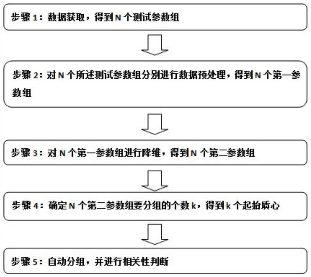
[0023] This embodiment provides a method for determining the correlation of wafer test parameters, and performs correlation determination for wafer test parameter groups under different test methods, such as figure 1 shown, including:
[0024] Step S1. Using N kinds of test methods to conduct wafer electrical tests to obtain test results, that is, to obtain N test parameter groups.
[0025] Step S2. Perform data preprocessing on each test parameter group to obtain N first parameter groups, so that the parameter distribution of each first parameter group conforms to normal distribution or lognormal distribution.
[0026] Step S3. Preset feature dimension g, where g is a positive integer; perform feature extraction and dimensionality reduction on the N first parameter groups, respectively, to obtain N second parameter groups, and the second parameter groups include g-dimensional feature data.
[0027] Step S4. Determine the number of N second parameter groups to be grouped, den...
Embodiment 2
[0031] In this embodiment, the method for data acquisition is specifically: acquiring N test parameter groups, each test parameter group is an electrical parameter measured under a test method, and different test parameter groups are obtained under different test methods Measured; each electrical parameter in the test parameter group corresponds to a test result obtained by performing an electrical test on a test unit at a position coordinate in the wafer.
[0032]In this embodiment, each test parameter group includes several electrical parameters, that is, several measured parameter values; each electrical parameter corresponds to a grain coordinate (x, y) to cover the entire wafer. All die to be tested; a die is a single unit die on a wafer. A test parameter group is a set of parameter values measured for all crystal grains in a wafer under a test method; in other embodiments, it can also be the test data after taking the median value of the test data of multiple wafers ....
Embodiment 3
[0035] In this embodiment, the method for data preprocessing specifically includes:
[0036] Separately for each test parameter group in turn: remove outliers, add missing data, test for normal distribution, and standardize.
[0037] Removing outliers refers to judging and deleting parameters in the test parameter group that exceed the preset data range as outliers. In this example, define (Q 1 -1.5IQR,Q 3 +1.5IQR) are outliers, IQR=Q 3 -Q 1 .
[0038] Adding missing data means that each set of test parameters includes a preset number of parameter values to correspond to the position coordinates in the wafer one by one, find out the position coordinates of missing electrical parameters, and add missing data by interpolation. In the present embodiment, the contour line is constructed by discrete points, and the existing grain coordinate range (x 1 ,y 1 ) to (x n ,y n ), using the resampling geometry to correct the parameter values, here a linear correction is used. ...
PUM
 Abstract
Description
Claims
Application Information