Path-based optical simulation device activation method and device, and terminal equipment

A device and optical technology, applied in devices and terminal equipment, and in the field of path-based optical simulation device activation methods, can solve the problems of difficulty in realizing the simulation process, and achieve the effect of reducing the amount of calculation and simplifying the simulation process

Pending Publication Date: 2022-01-14
海宁集成电路与先进制造研究院
View PDF0 Cites 0 Cited by
  • Summary
  • Abstract
  • Description
  • Claims
  • Application Information

AI Technical Summary

Problems solved by technology

Traditionally, optical system simulation is similar to the simulation process in electronic chip design. However, due to the differences in the physical properties of optical devices and electronic devices, and the unique nature of the propagation process of optical signals in optical systems, the realization of the simulation process High difficulty

Method used


Image

  • Path-based optical simulation device activation method and device, and terminal equipment
  • Path-based optical simulation device activation method and device, and terminal equipment
  • Path-based optical simulation device activation method and device, and terminal equipment

Examples


Embodiment Construction

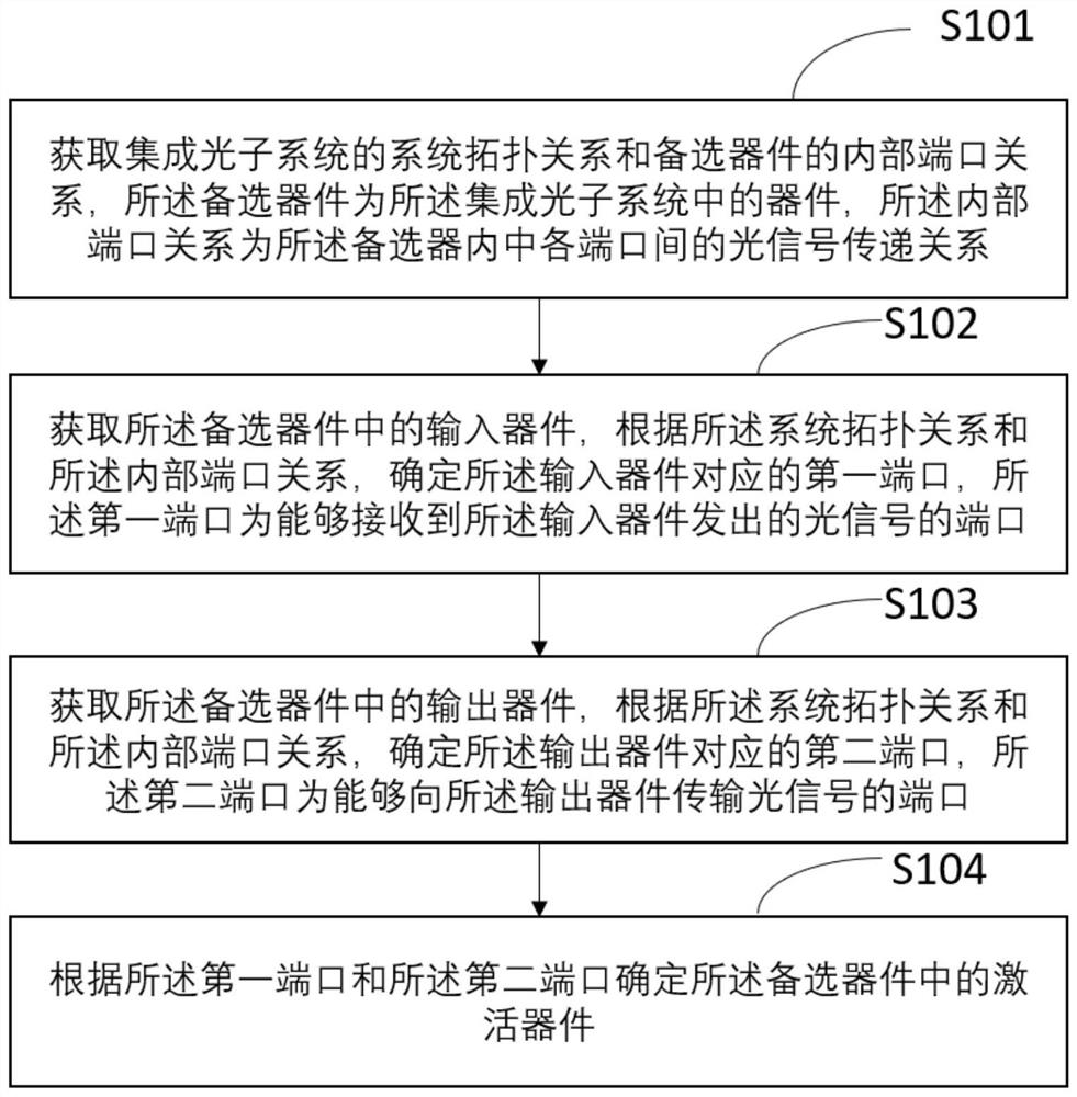
[0025] In the following description, specific details such as specific system structures and technologies are presented for the purpose of illustration rather than limitation, so as to thoroughly understand the embodiments of the present invention. It will be apparent, however, to one skilled in the art that the invention may be practiced in other embodiments without these specific details. In other instances, detailed descriptions of well-known systems, devices, circuits, and methods are omitted so as not to obscure the description of the present invention with unnecessary detail.

[0026] In order to illustrate the technical solutions of the present invention, specific examples are used below to illustrate.

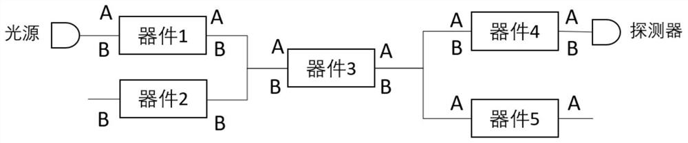
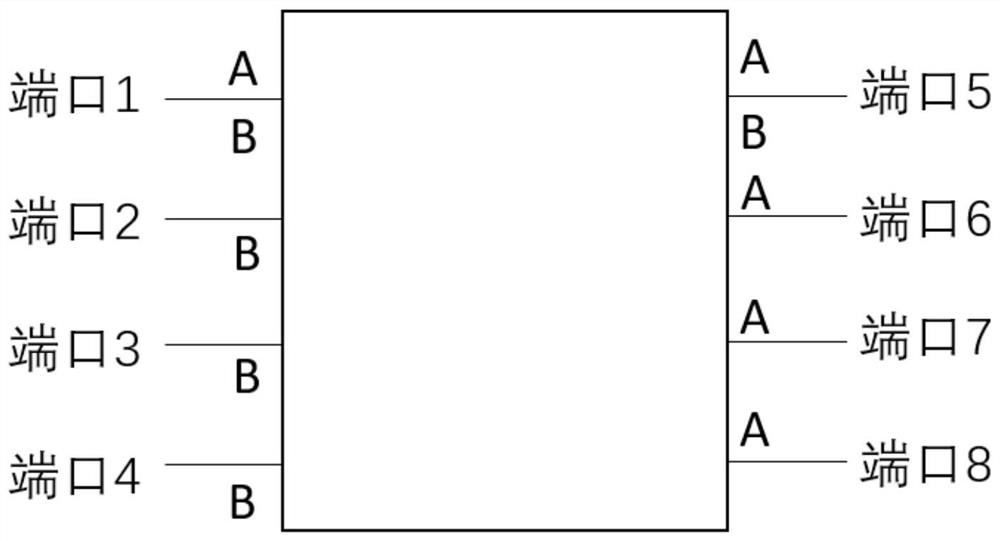
[0027] The path-based optical simulation device activation method provided by the embodiment of the present invention can be applied in the design process of photonic integrated chips. The above process will continuously call the behavior model of each device in the in...


PUM


Abstract

The invention is suitable for the field of photon integration, and provides a path-based optical simulation device activation method and device, and terminal equipment. The method comprises the steps that a system topological relation of an integrated photon system and an internal port relation of an alternative device are acquired; an input device and an output device in the alternative devices are obtained, a first port corresponding to the input device and a second port corresponding to the output device are determined according to the system topological relation and the internal port relation, the first port is a port capable of receiving optical signals sent by the input device, and the second port is a port capable of transmitting the optical signals to the output device; and an activated device in the alternative devices is determined according to the first port and the second port. According to the path-based optical simulation device activation method provided by the invention, the device needing to be activated in the integrated photon system can be simply, conveniently and quickly determined, so that the simulation process is effectively simplified, and the calculation amount is reduced.

Description

technical field [0001] The invention belongs to the technical field of computers, and in particular relates to a path-based optical simulation device activation method, device and terminal equipment. Background technique [0002] Photonic Integrated Circuit (PIC) technology is dedicated to the application of semiconductor technology to realize chip-based optical systems. Compared with traditional communication methods, optical communication has the advantages of high bandwidth and parallelism. Photonic chips based on photonic integration technology can play an important role in communication, fixed calculation and other fields, and optimize the communication bandwidth, power consumption performance and calculation of information systems. ability. [0003] In the design process of photonic integrated chips, the simulation of optical systems is essential. Traditionally, optical system simulation is similar to the simulation process in electronic chip design. However, due to ...

Claims


Application Information

Patent Timeline
Patent Type & Authority Applications(China)
IPC IPC(8): G06F30/398G06F17/16
CPCG06F30/398G06F17/16
Inventor 刘智帅赵复生王宇王硕张罗莎刘玉姝
Owner 海宁集成电路与先进制造研究院
Why Eureka
Try Eureka