LED packaging structure and manufacturing method thereof

A technology of LED packaging and manufacturing method, applied in electrical components, circuits, semiconductor devices, etc., can solve the problems of abnormal dispensing device, exposed light conversion layer, difficulty in mass production, etc., so as to facilitate dispensing and filling, and avoid blackening failure. , to ensure the effect of reliability

Pending Publication Date: 2022-01-21
APT ELECTRONICS
View PDF0 Cites 0 Cited by
  • Summary
  • Abstract
  • Description
  • Claims
  • Application Information

AI Technical Summary

Problems solved by technology

Due to the high concentration of fluorescent powder, the viscosity of the mixed fluorescent glue is relatively high, which may easily lead to the following problems: 1. The dispensing device is abnormal and it is difficult to produce in batches; 2. The fluorescent powder in the fluorescent glue is prone to agglomeration and the surface of the colloid is wrinkled; 3. After centrifugal sedimentation, a stable silica gel layer and light conversion layer structure cannot be formed, and the light conversion layer is exposed, resulting in the hydrolysis reaction between the fluoride phosphor powder in the fluorescent glue and the moisture in the air, resulting in blackening and failure
In order to solve the problem of high viscosity of fluorescent glue, the existing method is to use phosphor with particle size D50 less than 20 μm, which can improve the dispensing effect, and can control the phosphor layer to be covered by glue thickness less than 30 μm to ensure reliability, but This approach results in significantly lower package brightness than packages using large particle size phosphors

Method used


Image

  • LED packaging structure and manufacturing method thereof
  • LED packaging structure and manufacturing method thereof
  • LED packaging structure and manufacturing method thereof

Examples


Embodiment 1

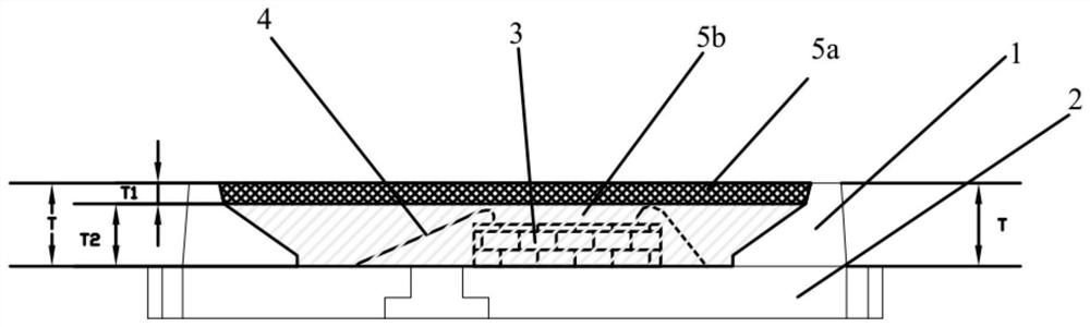
[0046] A LED packaging structure, such as figure 1 As shown, it includes a bracket, LED chips 3, wires 4 and fluorescent glue 5. The bracket includes a bracket cup 1 and a conductive substrate 2. The bracket cup 1 is bowl-shaped, and the bottom of the bracket cup 1 is fixed on the conductive substrate 2. surface. The LED chip 3 is fixed on the conductive substrate 2 and is located in the bracket cup 1; one end of the wire 4 is connected to the LED chip 3, and the other end is connected to the conductive substrate 2, so that the LED chip 3 and the conductive substrate 2 are electrically connected. Fluorescent glue 5 is filled in the bracket bowl cup 1, and the fluorescent glue 5 is composed of an upper layer of silica gel layer 5a and a lower layer of light conversion layer 5b, and the light conversion layer 5b is coated on the LED chip 3 to seal it in the bracket bowl cup 1, The silica gel layer 5a covers the upper surface of the light conversion layer 5b to isolate the light...

experiment example 1

[0057] Glue experiment.

[0058] Take the fluorescent glue in the examples and comparative examples respectively, put them into the glue dispenser, turn on the switch of the glue dispenser, fill the fluorescent glue into the bracket bowl, and observe the effect of glue dispensing. If the surface of the colloid is flat after dispensing, it means that the dispensing is normal. If there is agglomeration of phosphor powder, wrinkles on the surface of the colloid or other abnormal phenomena after dispensing, it means that the dispensing is abnormal. After dispensing, use a centrifugal device to centrifugally settle under the same conditions to observe the state of the colloid section.

[0059] Experimental results: the fluorescent glue of Example 1 is normally dispensed, and the surface of the colloid is smooth and smooth ( Figure 4 ), a stable silica gel layer and light conversion layer were formed after centrifugal sedimentation, and the surface of the light conversion layer wa...

experiment example 2

[0061] Package brightness experiment.

[0062] Experimental method: Seal the sample in the 2835 package, and use 100mA to light up the test. The test results are shown in Table 1.

[0063] Table 1. Brightness comparison of LED package structure

[0064]

[0065]

[0066] It can be seen from the above table that the package luminance of Example 1 and Comparative Example 1 are equivalent, obviously better than that of Comparative Example 2, the brightness of which is 2.8% and 2.4% higher respectively. Adding diluent can reduce the viscosity of fluorescent glue.


PUM

PropertyMeasurementUnit
particle diameteraaaaaaaaaa
thicknessaaaaaaaaaa

Abstract

The invention provides an LED packaging structure and a manufacturing method thereof, and relates to the technical field of LEDs. The LED packaging structure comprises a bracket which comprises a bracket bowl cup and a conductive substrate, wherein the bracket bowl cup is fixed on the conductive substrate; an LED chip which is fixed on the conductive substrate and is arranged in the bracket bowl cup; a wire which is arranged in the bracket bowl cup, so that the LED chip is electrically connected with the conductive substrate; and fluorescent glue which is filled in the bracket bowl cup. The fluorescent glue comprises a silica gel layer and a light conversion layer, the light conversion layer coats the LED chip, and the silica gel layer coats the outer surface of the light conversion layer, so that the light conversion layer is isolated from the external environment; the fluorescent glue is prepared from yellow-green fluorescent powder, fluoride fluorescent powder, silicon resin and a diluent; and the particle size D50 of the yellow fluorescent powder is 20-30 [mu] m, and the particle size D50 of the fluoride fluorescent powder is 20-40 [mu] m. The LED packaging structure is not prone to blackening and failure, and the packaging brightness can be guaranteed.

Description

technical field [0001] The invention relates to the technical field of LEDs, in particular to an LED packaging structure and a manufacturing method thereof. Background technique [0002] LED color temperature can be divided into low color temperature, medium color temperature and high color temperature. The low color temperature is below 3300K, the medium color temperature is 3300-8000K, and the high color temperature is above 8000K. The powder glue used in the existing 1000-2700K low color temperature LED packaging structure is relatively high, in which the phosphor powder accounts for more than 65% of the weight of the packaging glue, and the weight of the fluoride-containing phosphor accounts for more than 50% of the powder. Due to the high concentration of fluorescent powder, the viscosity of the mixed fluorescent glue is relatively high, which may easily lead to the following problems: 1. The dispensing device is abnormal and it is difficult to produce in batches; 2. Th...

Claims


Application Information

Patent Timeline
Patent Type & Authority Applications(China)
IPC IPC(8): H01L33/48H01L33/50H01L33/54
CPCH01L33/486H01L33/501H01L33/504H01L33/505H01L33/54H01L2933/0033H01L2933/0041
Inventor 蓝义安万垂铭朱文敏徐波曾照明肖国伟
Owner APT ELECTRONICS
Why Eureka
Try Eureka