Method for removing peak interference of electronic probe line analysis and application of method

An electronic probe and distribution map technology, which is applied to the use of wave/particle radiation for material analysis, material analysis, and measurement devices, can solve problems such as inaccurate N element distribution results, reduce environmental pollution, and achieve accurate detection results. Effect

Pending Publication Date: 2022-02-01
INST OF RES OF IRON & STEEL JIANGSU PROVINCE +1
View PDF0 Cites 0 Cited by
  • Summary
  • Abstract
  • Description
  • Claims
  • Application Information

AI Technical Summary

Problems solved by technology

[0004] Therefore, the problem to be solved by the present invention is that when electronic probes are used in the prior art to detect the distribution of N elements on the Ti alloy substrate, the results of the distribution of N elements on the Ti alloy substrate are inaccurate.

Method used


Image

  • Method for removing peak interference of electronic probe line analysis and application of method
  • Method for removing peak interference of electronic probe line analysis and application of method

Examples


Embodiment 1

[0022] A method for removing interference from electron probe line analysis peaks, comprising:

[0023] (1) The selected material is a sample that has been nitrided on a titanium alloy.

[0024] (2) Grinding and polishing the sample, according to the metallographic grinding and polishing steps, sequentially select 180#-800#-1200#-1500#-2000# sandpaper for polishing, and then finely polish with 1 μm diamond suspension to reach Electron probe analysis requirements.

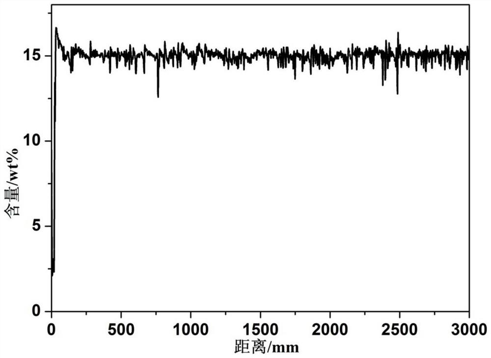
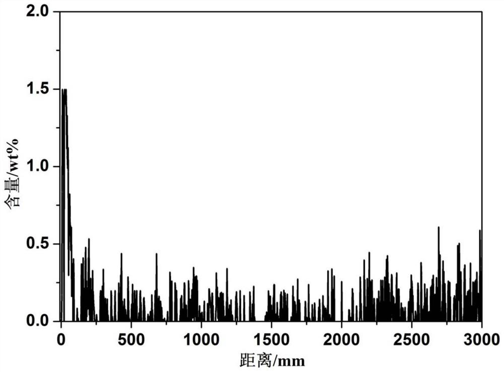
[0025] (3) Put the sample into the electronic probe sample chamber, wait until the vacuum value reaches 1.0×10 -3 At Pa, select the accelerating voltage as 10kV, the probe beam current as 100nA, the beam spot diameter as 1μm, the step diameter as 2μm, and the line analysis length as 3mm to determine the area to be measured. element and Ti element, until the end of the scan, the line distribution diagram of the N element obtained by scanning is as follows figure 1 shown.

[0026] (4) According to the formula show...


PUM


Abstract

The invention discloses a method for removing peak interference of electronic probe line analysis and application of the method. The method for removing the peak interference of the electronic probe line analysis comprises the following steps of: acquiring the intensity IN K alpha of an N element line distribution diagram on a to-be-detected sample by adopting an electronic probe, and acquiring the intensity ITi (N K alpha) of a Ti element and the intensity ITi K alpha of a Ti element line distribution diagram measured at the wavelength of an N element K alpha at the same time; and acquiring actual linear distribution content Nactual of the N element by adopting a data processing mode of deducting the peak interference of the Ti element. According to the method, the peak interference of the Ti element can be deducted, so that the distribution result of the N element on the Ti alloy matrix is calculated and processed, and the purpose of acquiring the linear distribution diagram for accurately representing the real content of the N permeation layer is achieved.

Description

technical field [0001] The invention relates to the field of material analysis, in particular to a method for removing the interference of electronic probe line analysis peaks and an application thereof. Background technique [0002] In recent years, the demand for the detection of light element N in electronic probes has been increasing, mainly because the heat treatment method of nitriding is adopted in the industry to increase the hardness and wear resistance of the workpiece. The traditional methods for detecting the thickness and trend of nitriding are hardness method and metallographic method. Among them, the hardness method cannot measure to the edge, which will lose the information of the edge of the sample. The metallographic method has judgment errors for samples whose nitriding layer interface is not obvious. Moreover, the first two methods cannot obtain the thickness and content distribution trend of the nitriding layer at the same time. At present, the best meth...

Claims


Application Information

Patent Timeline
Patent Type & Authority Applications(China)
IPC IPC(8): G01N23/225G01N23/2202
CPCG01N23/225G01N23/2202
Inventor 吴园园金传伟石丽丽张继明
Owner INST OF RES OF IRON & STEEL JIANGSU PROVINCE
Why Eureka
Try Eureka