High-frequency probe card for wafer testing

A high-frequency probe and wafer testing technology, applied in the field of high-frequency probe cards, can solve the problems of high cost, small probe size, easy to wear and even bending, etc., and achieve the effect of low maintenance cost

Active Publication Date: 2022-02-11
PROBELOGIC SHANGHAI CO LTD
View PDF18 Cites 0 Cited by
  • Summary
  • Abstract
  • Description
  • Claims
  • Application Information

AI Technical Summary

Problems solved by technology

[0003]However, the probes on the test probe card are prone to wear and even serious bending during the long-term test operation, which leads to the failure of the probes to work normally. There is an electrical connection between the testing machine and the integrated chip, and the probe is small in size, and it is difficult to detect the severely bent and worn probe visually, and it is easy to affect the subsequent integrated chip test results. When the existing test probe is damaged, it needs to be replaced as a whole, and the cost is high

Method used


Image

  • High-frequency probe card for wafer testing
  • High-frequency probe card for wafer testing
  • High-frequency probe card for wafer testing

Examples


Embodiment

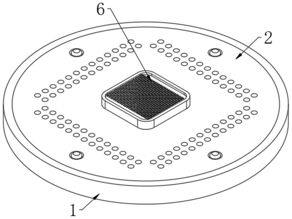
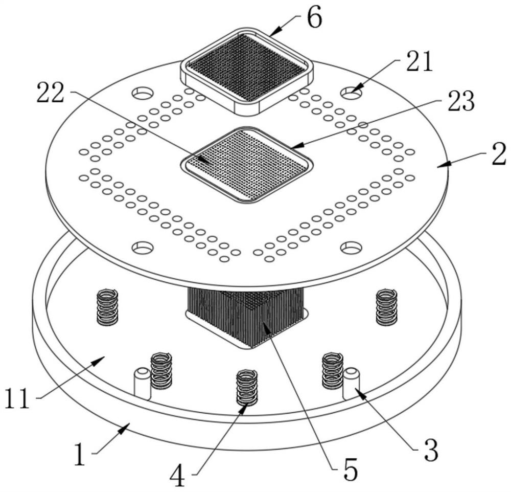
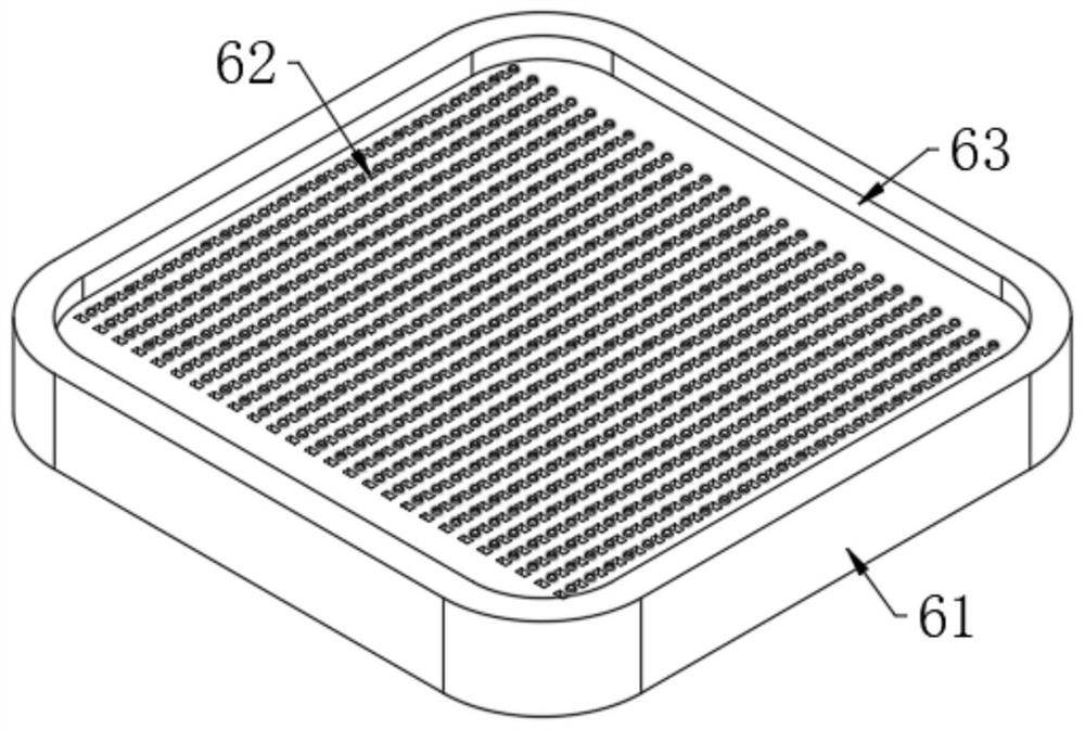
[0032] refer to Figure 1-10 , a high-frequency probe card for wafer testing is proposed in this embodiment, including a connection base 1, a panel 2 is slidably installed on the connection base 1, and a connection tester and an integrated chip signal are fixedly installed on the connection base 1. The probe group 5 of the contact, the probe group 5 runs through the panel 2 and is slidably connected with the panel 2, the panel 2 is detachably installed with a rectification assembly 6, the rectification assembly 6 is located outside the probe group 5, and the rectification assembly 6 is installed on The working state of the probe set 5 is detected at the upper end of the panel 2, and the probe set 5 is straightened and corrected when the correction assembly 6 is disassembled.

[0033] Specifically, when testing the integrated chip, the connecting base 1 and the testing machine are fixedly connected together, and then the testing machine drives the connecting base 1 and the pane...


PUM


Abstract

The invention belongs to the technical field of integrated circuit testing, and particularly relates to a high-frequency probe card for wafer testing, the high-frequency probe card comprises a connecting base, a panel is slidably mounted on the connecting base, a probe group for connecting a testing machine and an integrated chip signal contact is fixedly mounted on the connecting base, and the probe group penetrates through the panel and is slidably connected with the panel. A correction assembly is detachably installed on the panel and located on the outer side of the probe group. According to the invention, when a certain detection part of the probe group is bent or worn seriously and cannot be in normal contact with a certain signal contact of the integrated chip, the indication assembly gives out an indication, so that a user is reminded to maintain the probe group, and the test machine and the integrated chip can be normally conducted by the whole probe group; the correction assembly can correct the detection part which is abraded or bent seriously, it is ensured that the correction assembly can conduct the test machine and the integrated chip, overall replacement is not needed, and the maintenance cost is low.

Description

technical field [0001] The invention relates to the technical field of integrated circuit testing, in particular to a high-frequency probe card for wafer testing. Background technique [0002] Since the advent of smartphones, mobile data traffic has grown explosively. With the emergence of further intelligent, user-centric terminal devices and inter-device communication terminals in the future, this trend will be further accelerated, and the pursuit of faster speed will continue. , Communication technology changes have great requirements on surface acoustic wave filter chips. Compared with mobile phone shipments, with the development and changes of the communication era, the frequency bands to be covered also increase. Therefore, surface acoustic wave filter chips must be equipped, and all The amount to be carried also increases proportionally. The surface acoustic wave filter is an indispensable component in the operation of radio frequency, Wi-Fi, Bluetooth, and mobile com...

Claims


Application Information

Patent Timeline
Patent Type & Authority Applications(China)
IPC IPC(8): G01R1/073H01L21/66
CPCG01R1/07364H01L22/34
Inventor 鹿时领汤慧敏
Owner PROBELOGIC SHANGHAI CO LTD
Why Eureka
Try Eureka