Voltage sampling structure based on SGT-MOSFET

A voltage sampling, B-9 technology, applied in the direction of only measuring voltage, measuring current/voltage, circuits, etc., can solve the problems of poor voltage sampling followability, large application circuit size, and difficult voltage sampling, etc., to achieve good compatibility and reduce System cost, the effect of optimizing device compatibility

Active Publication Date: 2022-02-18
VANGUARD SEMICON CORP
View PDF6 Cites 0 Cited by
  • Summary
  • Abstract
  • Description
  • Claims
  • Application Information

AI Technical Summary

Problems solved by technology

Traditional sampling technology is mainly realized through peripheral components. These components may have problems such as poor compatibility with main devices, increased production costs, large application circuit size, and poor followa

Method used


Image

  • Voltage sampling structure based on SGT-MOSFET
  • Voltage sampling structure based on SGT-MOSFET
  • Voltage sampling structure based on SGT-MOSFET

Examples


Embodiment Construction

[0025] Embodiments of the present invention are described below through specific examples, and those skilled in the art can easily understand other advantages and effects of the present invention from the content disclosed in this specification. The present invention can also be implemented or applied through other different specific implementation modes, and various modifications or changes can be made to the details in this specification based on different viewpoints and applications without departing from the spirit of the present invention.

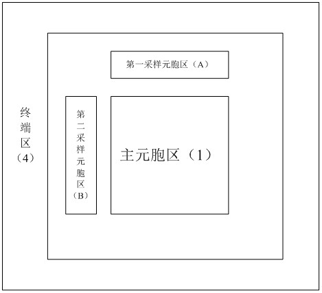
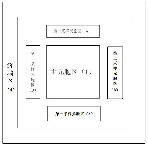
[0026] figure 1A schematic diagram of a voltage sampling structure based on SGT-MOSFET proposed by the present invention, including: SGT-MOSFET main cell area 1, with a groove, and a shielding gate is arranged in the groove; the first sampling cell area A, Set on one side of the main cell area of ​​the SGT-MOSFET, the first sampling cell area A has a groove, and a shielding gate is arranged in the groove; the second sampling cell area...


PUM


Abstract

The invention provides a voltage sampling structure based on an SGT-MOSFET. The structure comprises an SGT-MOSFET main cellular region, a first sampling cellular region and a second sampling cellular region. A source electrode of the SGT-MOSFET main cellular region is electrically connected with a source electrode of the first sampling cellular region and a source electrode of the second sampling cellular region; and the SGT-MOSFET main cellular region is not electrically connected with the shielding grid of the first sampling cellular region and the shielding grid of the second sampling cellular region, the shielding grid of the first sampling cellular region is electrically connected with the shielding grid of the second sampling cellular region, and the terminal area surrounds the SGT-MOSFET main cellular region, the first sampling cellular region and the second sampling cellular region. According to the voltage sampling structure based on the SGT-MOSFET provided by the invention, the voltage with the same change trend as the drain voltage of the device can be obtained, and sampling and feedback can be realized in time.

Description

technical field [0001] The invention belongs to the field of power semiconductor devices, in particular to a voltage sampling structure based on SGT-MOSFET. Background technique [0002] Power semiconductor devices are one of the important research contents in the field of semiconductors. They are mainly used in power processing units of modern electronic systems and are one of the key technologies in the fields of consumer electronics, industrial control and national defense equipment. In the high-voltage and power integrated circuits and systems related to power drives, it is necessary to detect the input / output performance and load conditions of high-voltage and power integrated circuits, so as to achieve real-time protection of circuits and systems, and to meet the intelligence of integrated circuits and systems , to effectively ensure the normal and reliable operation of the system. [0003] Power semiconductor devices face many failure situations in practical applicat...

Claims


Application Information

Patent Timeline
IPC IPC(8): H01L27/088H01L29/78G01R19/00
CPCH01L27/088H01L29/7813H01L29/7831G01R19/0084
Inventor 李伟聪姜春亮雷秀芳
Owner VANGUARD SEMICON CORP
Why Eureka
Try Eureka