

Film preparation method for improving surface shape of optical element
A technology for film preparation and optical components, applied in optical components, optics, ion implantation and coating, etc., can solve the problems of inappropriate optical components, increase processes and costs, and achieve the effect of reducing adverse effects and improving surface shape
Pending Publication Date: 2022-02-25
FUJIAN CASTECH CRYSTALS
View PDF0 Cites 0 Cited by
- Summary
- Abstract
- Description
- Claims
- Application Information
AI Technical Summary
Problems solved by technology
However, this method will increase the process and cost, and is not suitable for optical components with spectral requirements for non-mirror surfaces, so new methods are needed to improve the surface shape of optical components
Method used
View moreImage
Smart ImageViewing Examples

Examples
Embodiment 1
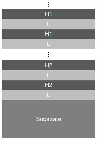
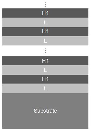
[0018] (1) Substrate treatment: Clean the substrate by ultrasonic method and dry it with isopropanol.
[0019] (2) Plating: use ion beam assisted deposition method, keep the temperature at 210°C for 40min, 1.8x10 -3 Under Pa vacuum degree, the following film system will be designed: 1.85L-1.98H2-1.99L-1.55H2-2.37L-1.39H2-2.32L-1.54H2-1.79L-0.74H2-0.99L-1.13H2-1.00L -0.79H2-1.06L-1.23H2-1.07L-0.81H2-0.92L-1.20H2-1.08L-0.90H1-0.88L-1.10H1-0.99L-0.95H1-0.99L-1.08H1-0.88L-0.93 H1-1.06L-1.11H1-0.90L-0.89H1-1.08L-1.09H1-0.89L-0.91H1-1.72L (H2 is hafnium oxide; H1 is tantalum pentoxide; L is silicon dioxide)
[0020] plated onto the substrate.
[0021] In this embodiment, the PV measured by the ZYGO interferometer is 0.12λ@633nm.
Login to View More PUM
 Abstract
The invention relates to a film preparation method for improving the surface shape of an optical element. Existing film stress is matched through a high-refractive-index film layer with tensile stress, the adverse effect of the film stress on the surface shape of the optical element is weakened, and thus the surface shape of the optical element is improved. According to the method, the surface shape of the optical element is remarkably improved, procedures can be reduced, and cost is reduced.
Description
technical field [0001] The invention belongs to the field of optical element processing, and specifically refers to a film preparation method for improving the surface shape of an optical element. Background technique [0002] As the most core optical mirror in the optical system, the quality of its surface shape directly affects the overall performance of the optical system. In high-energy laser systems, the requirements for the surface shape of single crystal silicon mirrors are also getting higher and higher. We generally use the peak-to-valley value (PV) measured by the interferometer to evaluate the surface shape of optical components. The smaller the PV, the higher the surface shape accuracy of the optical element. During the process of coating the surface of the optical element with a thin film, the optical element will be deformed due to the stress of the film, which will have an adverse effect on the surface shape. The current solution is generally non-mirror coa...
Claims
Login to View More Application Information
Patent Timeline
 IPC IPC(8): C23C14/10C23C14/06C23C14/08C23C14/22G02B1/10
CPCC23C14/10C23C14/0694C23C14/083C23C14/221G02B1/10
Inventor钟强马新建吴先云廖洪平陈伟陈秋华
OwnerFUJIAN CASTECH CRYSTALS