Resistor layout arrangement structure applied to high-precision and high-common-mode differential amplifier and trimming method

A differential amplifier, high-precision technology, used in special data processing applications, instruments, electrical digital data processing, etc. The effect of solving the poor initial matching degree, reducing the deviation and reducing the cost of trimming

Pending Publication Date: 2022-02-25
CHONGQING ZHONGKE YUXIN ELECTRONICS +1
View PDF0 Cites 0 Cited by
  • Summary
  • Abstract
  • Description
  • Claims
  • Application Information

AI Technical Summary

Problems solved by technology

It is impossible to meet the requirements of high matching degree of dual resistors, small trimming traces, and small occupied area at the same time.

Method used


Image

  • Resistor layout arrangement structure applied to high-precision and high-common-mode differential amplifier and trimming method
  • Resistor layout arrangement structure applied to high-precision and high-common-mode differential amplifier and trimming method
  • Resistor layout arrangement structure applied to high-precision and high-common-mode differential amplifier and trimming method

Examples


Embodiment 1

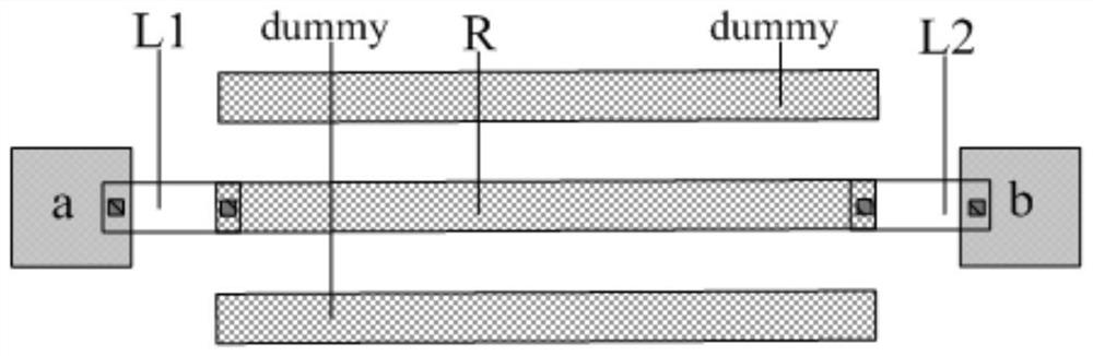
[0043] See Figures 1 to 7 A resistance layout arrangement applied to high-precision high-interstitial difference amplifiers, including two resistance arrays different from resistance. Among them, the resistance array having a small resistance is the first resistance array, and the resistive array having a large resistance is listed as a second resistance array.

[0044] The first resistor array and a second resistor array are connected by a metal wire.

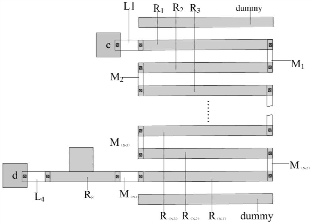
[0045] The second resistor array includes a series (N-1) strip rectangular resistance and a repairable backpack resistor R. N . (N-1) strip rectangular resistance is recorded as R 1 R 2 , ..., r N-1 . N is a resistance ratio of the second resistance array and the first resistance array.

[0046] The first resistor array is a rectangular resistance, and the resistance value is reserved as R.

[0047] The resistance of the second resistor array is N * R.

[0048] (N-1) Stand-shaped rectangular resistance is placed in parallel.

[00...

Embodiment 2

[0059] A resistance layout arrangement applied to high-precision high-interstitial difference amplifiers, including two resistance arrays of different resistance. Among them, the resistance array having a small resistance is the first resistance array, and the resistive array having a large resistance is listed as a second resistance array.

[0060] The first resistor array and a second resistor array are connected by a metal wire.

[0061] The second resistor array includes a series (N-1) strip rectangular resistance and a repairable backpack resistor R. N . (N-1) strip rectangular resistance is recorded as R 1 R 2 , ..., r N-1 . N is a resistance ratio of the second resistance array and the first resistance array.

Embodiment 3

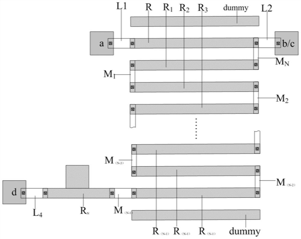
[0063] A resistance layout arrangement applied to a high-precision high-interstitial difference amplifier, the main structure is shown in Example 2, wherein the first resistor array is a rectangular resistance and a resistance value is R.


PUM


Abstract

The invention discloses a resistor layout arrangement structure applied to a high-precision and high-common-mode differential amplifier and a trimming method. The resistor layout arrangement structure comprises two resistor arrays with different resistance values. The trimming method comprises the steps of 1) measuring the actual resistance value of the first resistor array; 2) setting a trimming target value of a second resistor array, and recording the trimming target value as N * R; 3) measuring the actual resistance value of the second resistor array; 4) performing laser trimming on a coarse adjustment area of a trimmable backpack resistor RN in the second resistor array; and 6) performing laser trimming on the fine adjustment area of the trimmable backpack resistor RN in the second resistor array, and returning to the step 7). According to the invention, the layout of the two resistors is specially arranged, so that the deviation of the two resistors in the processing process is reduced, the initial matching degree of the two resistors is improved, and the higher resistor matching degree can be achieved, the trimming cost is reduced and the resistor stability is improved under the condition that only one resistor is trimmed and the trimming area of the resistor is small.

Description

Technical field [0001] The present invention relates to the field of integrated circuits, in particular a resistance layout arrangement for high precision high coordinating difference amplifiers and modulation methods. Background technique [0002] Laser Tuning Metal Thin Film Resistance is widely used in circuits such as precision instrumentation amplifiers, differential amplifiers, etc. During the process, photolithography, etching, packaged scribe, etc., can affect the stability and accuracy of the resistance. The differential amplifier requires a higher resistance value and a very high resistance matching to meet the demand for high performance parameters. The general metal thin film resistance is in the process of processing and packaging, and the resistance matching deviation has a maximum of 20%. The longer the trace of repair, the worse the matching resistance of the modulation resistance, the higher the resistance value, the larger the resistance, and the impact of stres...

Claims


Application Information

Patent Timeline
Patent Type & Authority Applications(China)
IPC IPC(8): G06F30/392
CPCG06F30/392
Inventor 杨法明朱坤峰欧宏旗钟怡税国华徐磊殷万军张广胜
Owner CHONGQING ZHONGKE YUXIN ELECTRONICS
Why Eureka
Try Eureka