On chip wafer alignment sensor
A technology of sensor equipment and optical devices, which is applied in the direction of instruments, photoplate-making process of pattern surface, measuring device, etc., and can solve the problem of not supporting alignment grating spacing and so on
- Summary
- Abstract
- Description
- Claims
- Application Information
AI Technical Summary
Problems solved by technology
Method used
Image

Examples
Embodiment Construction
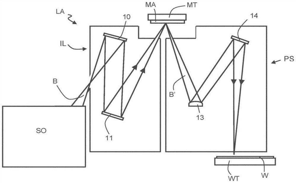
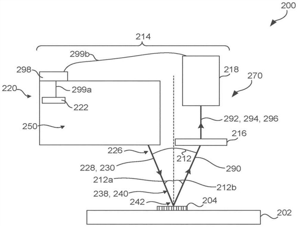
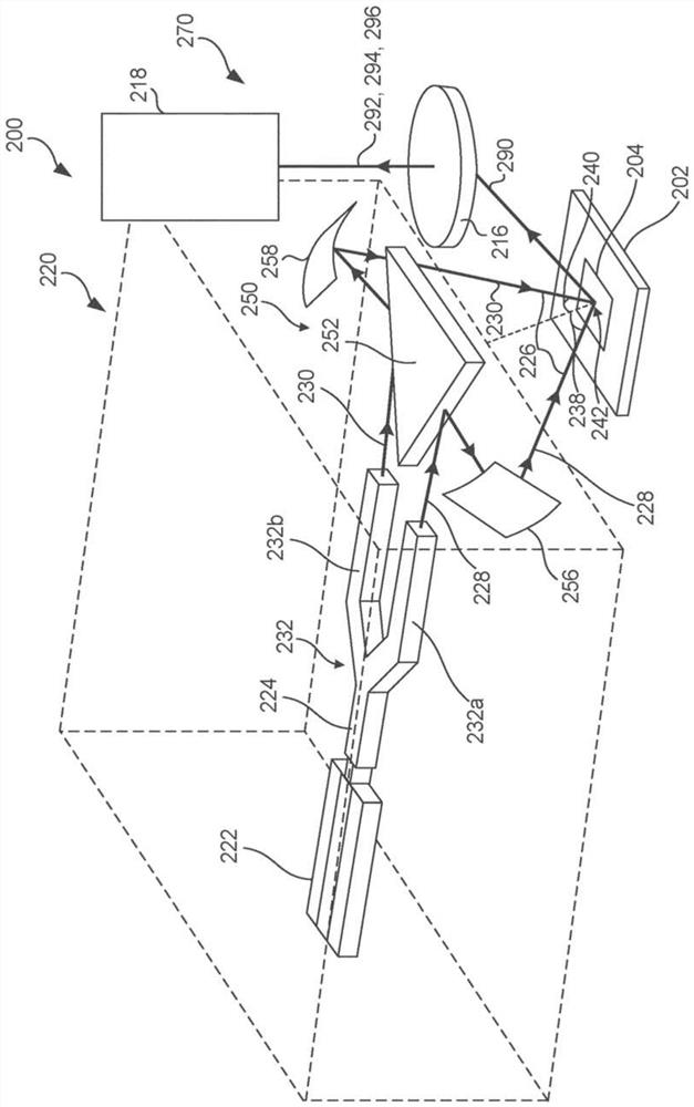
[0028] This specification discloses one or more embodiments that incorporate the features of this invention. The disclosed embodiments are merely illustrative of the invention. The scope of the invention is not limited to the disclosed embodiments. The invention is defined by the claims appended hereto.
[0029] The described embodiments and references in this specification to "one embodiment," "an embodiment," "example embodiment," etc. indicate that the described embodiment may include a particular feature, structure, or characteristic, but each embodiment may The specific features, structures or characteristics need not be included. Moreover, these phrases are not necessarily referring to the same embodiment. In addition, when a particular feature, structure or characteristic is described in conjunction with an embodiment, it is to be understood that it is within the purview of those skilled in the art to implement such feature, structure or characteristic in combination...
PUM
| Property | Measurement | Unit |
|---|---|---|
| Wavelength | aaaaa | aaaaa |
Abstract
Description
Claims
Application Information