FDSOI silicon epitaxial growth process optimization method
A technology of process optimization and silicon epitaxy, which is applied in the manufacture of electrical components, circuits, semiconductors/solid-state devices, etc., can solve the problems of excessive loss of top-layer silicon and the inability of epitaxial growth of top-layer silicon to achieve the goal of making up for loss and increasing thickness Effect
- Summary
- Abstract
- Description
- Claims
- Application Information
AI Technical Summary
Problems solved by technology
Method used
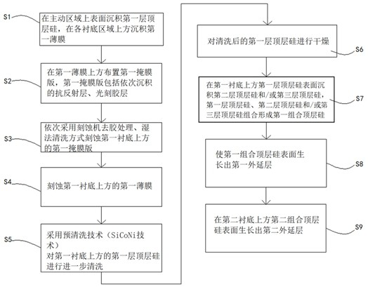
Image

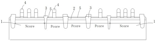
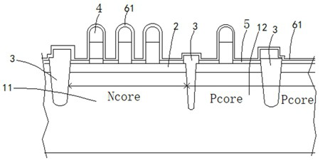
Examples
Embodiment Construction
[0054] In order to enable those skilled in the art to better understand the solutions of the present invention, the following will clearly and completely describe the technical solutions in the embodiments of the present invention in conjunction with the drawings in the embodiments of the present invention. Obviously, the described embodiments are only It is an embodiment of a part of the present invention, but not all embodiments. Based on the embodiments of the present invention, all other embodiments obtained by persons of ordinary skill in the art without making creative efforts shall fall within the protection scope of the present invention.
[0055] It should be noted that the terms "comprising" and "having" in the description and claims of the present invention and the above drawings, as well as any variations thereof, are intended to cover a non-exclusive inclusion, for example, including a series of steps or units A process, method, device, product or device is not ne...
PUM
| Property | Measurement | Unit |
|---|---|---|
| Deposition thickness | aaaaa | aaaaa |
Abstract
Description
Claims
Application Information
 - Generate Ideas
- Intellectual Property
- Life Sciences
- Materials
- Tech Scout
- Unparalleled Data Quality
- Higher Quality Content
- 60% Fewer Hallucinations
Browse by: Latest US Patents, China's latest patents, Technical Efficacy Thesaurus, Application Domain, Technology Topic, Popular Technical Reports.
© 2025 PatSnap. All rights reserved.Legal|Privacy policy|Modern Slavery Act Transparency Statement|Sitemap|About US| Contact US: help@patsnap.com