Test assembly capable of avoiding thermal influence in linear welding spot electromigration process and manufacturing method thereof

A technology for testing components and linear welding, which is applied in the direction of electronic circuit testing, test sample preparation, and electrical measurement, which can solve problems such as uneven thermal stress and melting of solder joints, and achieve the effect of reducing experimental errors

Pending Publication Date: 2022-03-08
BEIJING UNIV OF TECH
View PDF0 Cites 0 Cited by
  • Summary
  • Abstract
  • Description
  • Claims
  • Application Information

AI Technical Summary

Problems solved by technology

The solder joints are bonded to the PCB (Printed circuit boards), and at least one side is completely in contact with the PCB board. When the solder joints pass a large current for a long time, the thermal stress will be uneven. In severe cases, the solder joints may melt
At present, PCB is often used as the substrate for carrying linear solder joints in electromigration research. However, in this way, since the solder joints are directly pasted on the substrate, three sides are cooled by air, and one side is blocked by the PCB board, which is prone to the above-mentioned uneven thermal stress. Case

Method used


Image

  • Test assembly capable of avoiding thermal influence in linear welding spot electromigration process and manufacturing method thereof
  • Test assembly capable of avoiding thermal influence in linear welding spot electromigration process and manufacturing method thereof

Examples


Embodiment 1

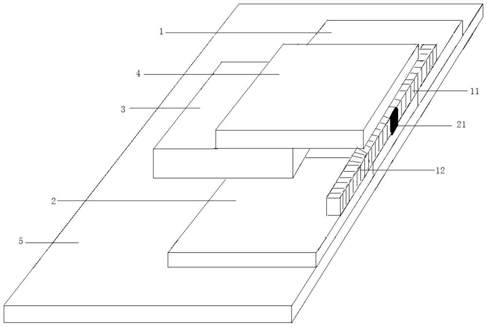
[0033] The first embodiment is described by taking the production of a Cu / Sn3.0Ag0.5Cu / Cu butt single crystal joint with uniform grain orientation, a cross-sectional size of 300 μm×300 μm, and a weld width of 300 μm as an example.

[0034] Such as figure 1 As shown, the test assembly for avoiding the thermal influence of the linear solder joint electromigration process according to the embodiment of the present application is characterized in that it includes a linear butt welding copper rod, a base plate 5 and a structural plate. Wherein, the linear butt welding copper rod comprises a linear welding point 21, a first copper rod 11 and a second copper rod 12; It is welded and connected with the second copper rod 12; the structural plate wraps the linear butt welding copper rod, the cross section of the linear butt welding copper rod is rectangular, and only one side of the linear butt welding copper rod is visible; the base plate 5 is used to carry the structural plate.

[00...

Embodiment 2

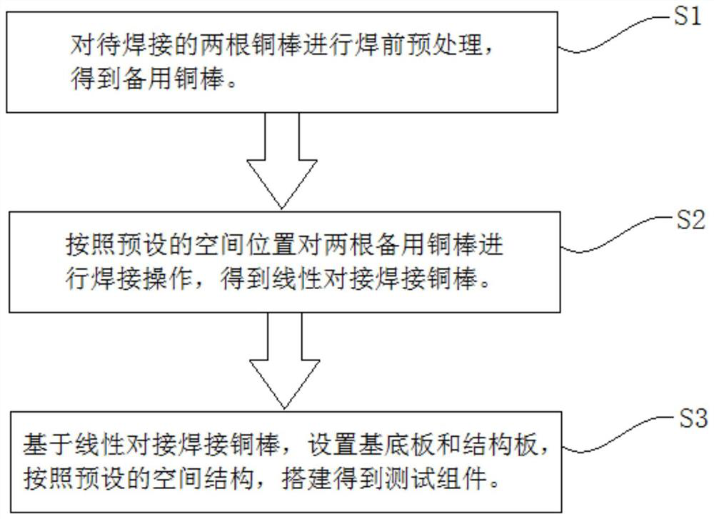
[0042] Such as figure 2 As shown, it is a schematic flow chart of the test component manufacturing method for avoiding the thermal influence of the linear solder joint electromigration process in Embodiment 2 of the present application, which mainly includes the following steps:

[0043] S1. Perform pre-welding pretreatment on the two copper rods to be welded to obtain spare copper rods. Pre-welding pretreatment mainly includes the size selection of copper rods, and the use of appropriate methods to remove the attachments on the surface of copper rods.

[0044] S2. Use solder paste to weld two spare copper rods according to the preset spatial position to obtain linear butt welded copper rods; the selection of solder paste should be based on the target solder joint composition, the spatial position of the copper rods It should be determined according to the size of the target test component and the requirements of the electromigration test. Further, manual grinding may be us...


PUM


Abstract

The invention discloses a test assembly capable of avoiding thermal influence in an electromigration process of a linear welding spot and a manufacturing method thereof. The test assembly comprises a linear butt welding copper rod, a base plate and a structural plate, the linear butt welding copper bar comprises a linear welding spot, a first copper bar and a second copper bar; the linear welding spot is located between the first copper bar and the second copper bar and is in welded connection with the first copper bar and the second copper bar; the structural plate wraps the linear butt welding copper bar, the section of the linear butt welding copper bar is rectangular, and only one side face of the linear butt welding copper bar is visible; the base plate is used for bearing the structural plate. According to the method, the difficulty that thermal stress generated by one-dimensional linear welding spots during electrification in a traditional method is not uniform is overcome, expression of evolution behaviors of interface intermetallic compounds in the electromigration process is facilitated, and the reliability of butt joints of the linear welding spots can be accurately evaluated; furthermore, experimental errors caused by thermal stress to the welding spots are greatly reduced, and the requirement that only the power-on time needs to be considered for the unique variable during electromigration testing is met.

Description

technical field [0001] The application belongs to the technical field of material preparation and connection, and in particular relates to a test component and a manufacturing method thereof for avoiding the thermal influence of a linear solder joint electromigration process. Background technique [0002] Solder joints are an integral part of microelectronic interconnects, serving as both mechanical connections and electrical signal transmissions. At present, the microelectronic packaging space is reduced, and the heat generation of the chip is intensified. On the one hand, affected by the current, the interface intermetallic compound ( IntermetallicCompounds, IMCs) layer morphology, size, crystal orientation and thickness have more and more serious impact on the reliability of solder joints. cavities, leading to microcracks. Therefore, a considerable amount of experimental work has been devoted to the study of the morphology changes of solder joints after electrical treat...

Claims


Application Information

Patent Timeline
Patent Type & Authority Applications(China)
IPC IPC(8): G01R31/28G01N13/02G01N1/28B23K3/08B23K1/20B23K1/00
CPCG01R31/2806G01N13/02G01N1/28B23K1/00B23K1/20B23K3/08G01N2013/0225
Inventor 汉晶晋学轮郭福马立民孟洲曹恒李子萱贾强周炜籍晓亮王乙舒王晓露
Owner BEIJING UNIV OF TECH
Why Eureka
Try Eureka