
A semiconductor packaging method

A packaging method and semiconductor technology, which is applied in the direction of semiconductor devices, semiconductor/solid-state device manufacturing, semiconductor/solid-state device components, etc., can solve the problems of limiting product-related performance improvement and high cost, and avoid pad modification or Effect of RDL process

Active Publication Date: 2022-05-24
SHENZHEN SIPTORY TECH CO LTD
View PDF8 Cites 0 Cited by
  • Summary
  • Abstract
  • Description
  • Claims
  • Application Information

AI Technical Summary

Problems solved by technology

[0005] On the one hand, the wire bonding process limits the improvement of product-related performance. On the other hand, the new blind via interconnection process requires additional complex and costly pad modification or RDL on existing conventional chips. How to effectively solve the above problems is worth studying.

Method used


Image

  • A semiconductor packaging method
  • A semiconductor packaging method
  • A semiconductor packaging method

Examples


Embodiment 1

[0069] A semiconductor packaging method, comprising:

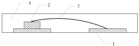
[0070] Step A. Mount the chip 2 on the lead frame 1, and use the wire bonding process to make the wire bonding terminal structure 3 on the upper surface AL pad 21 of the chip 2; the wire bonding terminal structure 3 includes a tight connection from bottom to top The wire bonding pad contacts the ball 31, the transition connection table 32 and the wire head 33; Figure 13a and Figure 7 shown.

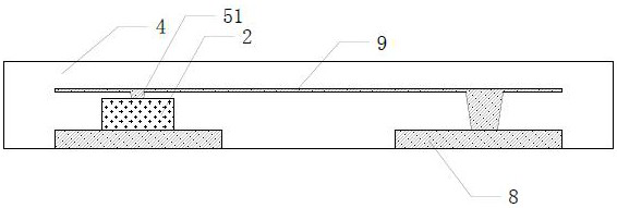
[0071] Step B. The lead frame 1 produced by the wire-bonding terminal structure 3 is plastic-sealed or press-sealed for the first time, so as to realize the complete wrapping of the chip 2 and the wire-bonding terminal structure 3, and the top surface height of the wrapping layer 4 exceeds the height of the wire bonding terminal structure 3. The top surface of the wire end structure 3 is 20~50 μm; combined Figure 13b shown.

[0072] Step C. Thin the wrapping layer 4 until the wire bonding pad contact ball 31 is exposed, and rem...

Embodiment 2

[0075] A semiconductor packaging method, comprising:

[0076] Step A. Mount the chip 2 on the lead frame 1, and use the wire bonding process to make the wire bonding terminal structure 3 on the upper surface AL pad 21 of the chip 2; the wire bonding terminal structure 3 includes a tight connection from bottom to top The wire bonding pad contacts the ball 31, the transition connection table 32 and the wire head 33; Figure 13a and Figure 7 shown.

[0077] Step B. The lead frame 1 produced by the wire-bonding terminal structure 3 is plastic-sealed or press-sealed for the first time, so as to realize the complete wrapping of the chip 2 and the wire-bonding terminal structure 3, and the top surface height of the wrapping layer 4 exceeds the height of the wire bonding terminal structure 3. The top surface of the wire end structure 3 is 20~50 μm; combined Figure 13b shown.

[0078] Step C. Thin the wrapping layer 4 until the wire bonding pad contact ball 31 is exposed, and rem...

Embodiment 3

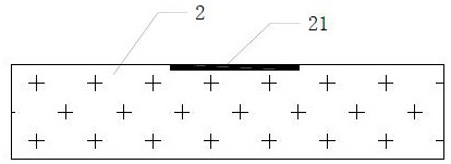
[0087] In this embodiment, the wire used in the wire bonding process is a variable-diameter wire, and the variable-diameter wire includes N or more ball-binding units 6 connected to each other, and each ball-binding unit includes a wire head 61 and a diameter-reducing part 62 And the joint part 63, the diameter of the wire head 61 and the joint part 63 is equal to the diameter of the wire, the diameter of the reducing part 62 is large and the two ends are small, and the maximum diameter of the reducing part 62 is 2~4 times the diameter of the wire. Figure 14 shown.

[0088] N is a natural number, and N is greater than or equal to 10.

[0089] The diameter reducing portion 62 includes a middle main body ball 621 and transition connection balls 622 on both sides. When making the wire-bonding end structure 3, the middle main body ball 621 becomes the main body of the wire bonding pad contacting ball 31, and the transition connection balls 622 are melted respectively. The two si...


PUM

PropertyMeasurementUnit
thicknessaaaaaaaaaa
thicknessaaaaaaaaaa

Abstract

The invention relates to a semiconductor packaging method, comprising: attaching a chip on a lead frame, and adopting a wire bonding process to manufacture a wire bonding terminal structure on the AL pad on the upper surface of the chip; the wire bonding terminal structure includes from bottom to bottom The contact ball of the bonding pad, the transition connection platform and the wire head are tightly connected on the upper surface; the first plastic packaging or press-fit packaging is carried out to realize the full wrapping of the chip and the wire bonding terminal structure, and the height of the top surface of the wrapping layer exceeds the wire bonding end The top surface of the head structure is 20~50μm; the coating layer is thinned until the contact ball of the bonding pad is exposed, the transition connection platform and the wire head are removed, and the modification of the AL pad to the gold ball or copper ball is realized, and the follow-up Packaging process. On the one hand, this method can avoid the limitation of the wire bonding process on the improvement of product-related performance, and on the other hand, it can avoid the complicated and high-cost pad modification or RDL process. The present invention also provides the packaging structure obtained by the above method and Packaging products.

Description

technical field [0001] The invention relates to the technical field of semiconductor packaging, in particular to a semiconductor packaging method and packaging structure. Background technique [0002] As a traditional semiconductor packaging process, the wire bonding process has been widely used in chip packaging and processing in various fields ( figure 1 , traditional wire bonding product packaging structure), including lead frame 1, chip 2, lead 7 and wrapping layer 4. However, with the increasingly high performance requirements of products: for example, the internal resistance of the product requires the parasitic internal resistance of the package to become smaller and smaller, and the heat dissipation of the product requires the heat dissipation capability of the package to become stronger and stronger. The wire bonding process (wire bonding) The wire diameter under processing (the diameter of the lead 7, which is usually 20-30 μm) is generally small, which becomes a ...

Claims


Application Information

Patent Timeline
Patent Type & Authority Patents(China)
IPC IPC(8): H01L21/48H01L23/488
CPCH01L21/4814H01L23/488H01L2224/18H01L2924/181H01L2224/48091H01L2924/00012H01L2924/00014H01L23/3107H01L23/495H01L24/03H01L24/05H01L24/19H01L24/24H01L2224/0384H01L2224/05557H01L2224/19H01L2224/24246
Inventor 邵冬冬
Owner SHENZHEN SIPTORY TECH CO LTD
Learn More