Semiconductor structure and forming method thereof

A semiconductor and conductive structure technology, applied in semiconductor devices, semiconductor/solid-state device manufacturing, transistors, etc., can solve problems such as the need to improve the reliability of semiconductor structures, and achieve the effect of reducing the risk of exposure, increasing the width, and improving the blocking ability.

Pending Publication Date: 2022-03-11
SEMICON MFG INT (SHANGHAI) CORP +1
View PDF0 Cites 0 Cited by
  • Summary
  • Abstract
  • Description
  • Claims
  • Application Information

AI Technical Summary

Problems solved by technology

[0004] However, the reliability of semiconductor structures formed by existing technologies needs to be improved

Method used


Image

  • Semiconductor structure and forming method thereof
  • Semiconductor structure and forming method thereof
  • Semiconductor structure and forming method thereof

Examples


Embodiment Construction

[0037]As mentioned in the background, the reliability of the semiconductor structure still needs to be improved. The reason why the reliability of the semiconductor structure is poor will be described in detail below with reference to the accompanying drawings.

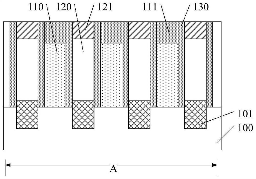
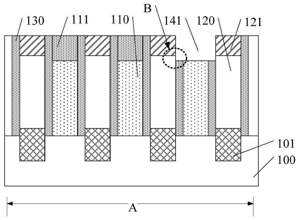
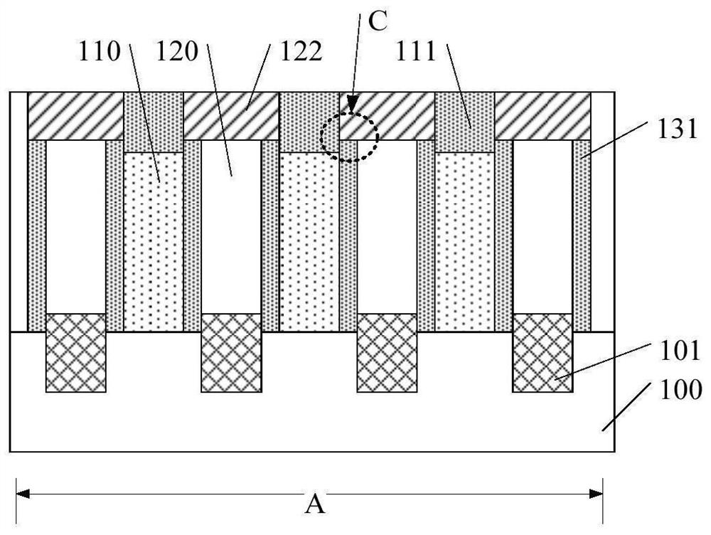
[0038] Figure 1 to Figure 2 It is a schematic cross-sectional structure diagram of each step of a method for forming a semiconductor structure.

[0039] Please refer to figure 1 , a substrate 100 is provided, the substrate 100 includes an active region A, and the substrate 100 has several mutually separated fins (not shown); on the substrate 100, a plurality of gate structures 110 across the fins are formed, located at the gate The source-drain doped regions 101 on both sides of the structure 110, the gate protection structure 111 located on the top surface of the gate structure 110, the conductive structure 120 located on the surface of the source-drain doped region 101, and the interconnect protection structure lo...


PUM

PropertyMeasurementUnit
thicknessaaaaaaaaaa
poweraaaaaaaaaa

Abstract

The invention discloses a semiconductor structure and a forming method thereof, and the method comprises the steps: providing a substrate; a plurality of source-drain structures, a plurality of gate structures and a first protection structure are formed, the source-drain structures are located in the portions, on the two sides of the gate structures, of the substrate, the gate structures are located on the substrate, each gate structure comprises a gate electrode layer, and the first protection structure is located on the top face of the gate electrode layer; forming a plurality of first conductive structures on the substrate, wherein the first conductive structures are located on the source and drain structures on at least one side of the gate structure; after the first conductive structure is formed, a second protection structure and a first side wall are formed, the second protection structure is located on the top face of the first conductive structure, and the first side wall is located between the first protection structure and the second protection structure. Therefore, the reliability of the semiconductor structure is improved.

Description

technical field [0001] The invention relates to the field of semiconductor manufacturing, in particular to a semiconductor structure and a forming method thereof. Background technique [0002] With the rapid development of semiconductor manufacturing technology, semiconductor devices are developing towards higher element density and higher integration. Devices, as the most basic semiconductor devices, are currently being widely used. [0003] Generally, in the manufacturing process of semiconductor devices, by forming a plug (Diffusion Contact) electrically connected to the source-drain doped layer in the active region, and forming a plug (Gate Contact) electrically connected to the gate outside the active region Contact), realize the electrical connection between the semiconductor device and the external circuit, and at the same time, increase the distance between the plugs electrically connected to the source-drain doped layer and the plugs electrically connected to the g...

Claims


Application Information

Patent Timeline
Patent Type & Authority Applications(China)
IPC IPC(8): H01L27/088H01L21/8234
CPCH01L27/0886H01L21/823431H01L21/823475
Inventor 郑二虎张海洋
Owner SEMICON MFG INT (SHANGHAI) CORP
Why Eureka
Try Eureka