Semiconductor process chamber

A process chamber and semiconductor technology, applied in metal material coating process, gaseous chemical plating, coating, etc., can solve the problem of inconsistent wafer exhaust pressure, exhaust uniformity of exhaust system, film thickness and uniformity , Affect the film thickness and uniformity and other issues to achieve the effect of ensuring circumferential uniformity

Pending Publication Date: 2022-03-18
BEIJING NAURA MICROELECTRONICS EQUIP CO LTD
View PDF6 Cites 1 Cited by
  • Summary
  • Abstract
  • Description
  • Claims
  • Application Information

AI Technical Summary

Problems solved by technology

Similarly, the exhaust uniformity of the exhaust system will also have a significant impact on the thickness and uniformity of the film
[0004] In the existing atomic layer deposition equipment, due to the limitations of the chamber structure and hardware such as the heating base, the exhaust system is usually placed eccentrically, resulting in inconsistent exhaust pressure around the wafer, and the exhaust gas flow field along the circumference of the process chamber uneven distribution, which affects the thickness and uniformity of the film

Method used


Image

  • Semiconductor process chamber
  • Semiconductor process chamber
  • Semiconductor process chamber

Examples


Embodiment approach

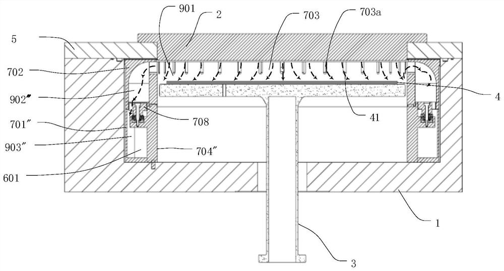
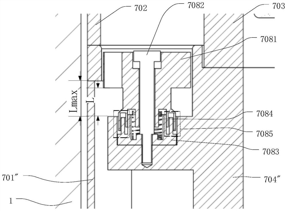
[0046] As an optional embodiment of the present invention, the thickness of the top wall (the baffle ring 7045) of the lower air guide is 5-15mm, and 12-36 air guide through-holes 7043 are formed on the top wall of the lower air guide. , preferably 18 air guide through holes 7043 are formed. The thickness of the plugging portion 7081d corresponds to the thickness of the top wall (baffle ring 7045) of the lower air guide, and each plugging portion 7081d is formed with 4 to 12 air guide holes 7081a, preferably 6 air guide holes 7081a. The diameter of the pores 7081a is 2 mm to 5 mm, preferably 3 mm.

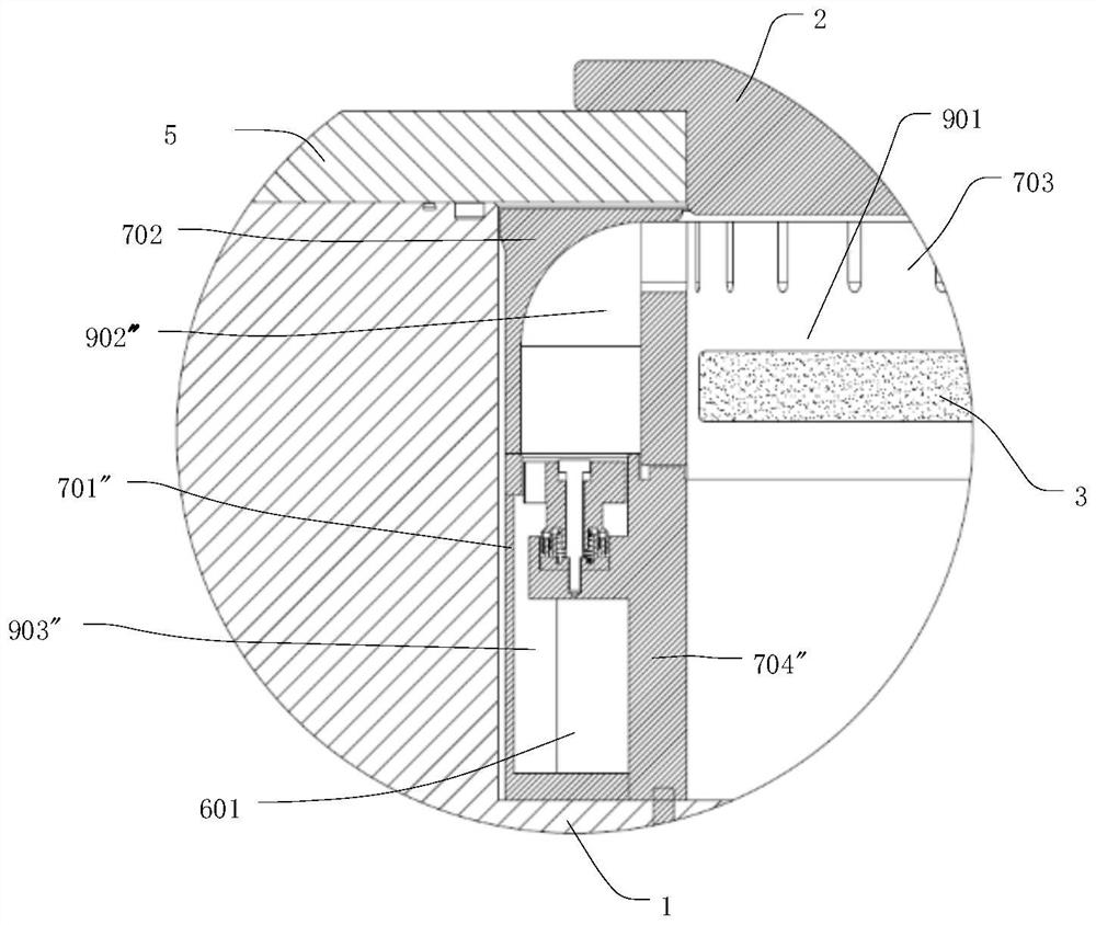
[0047] As an optional embodiment of the present invention, such as Figure 1 to Figure 6 As shown, the lower air guide includes a baffle ring 7045, an annular bottom plate, a component support ring 704" and a lower shield ring (Lower shield) 701", and the lower shield ring 701" is coaxially sleeved on the outside of the component support ring 704", The outer edge (that is, the ou...


PUM


Abstract

A semiconductor process chamber provided by the present invention comprises a cavity, a base and a gas guide structure, the gas guide structure comprises an upper gas guide part and a lower gas guide part, an upper gas guide cavity of the upper gas guide part is used for receiving gas from the periphery of the base, an annular opening is formed in the bottom of the upper gas guide part, and the bottom of the lower gas guide part is communicated with an exhaust port 601. A plurality of air guide through holes for communicating the upper air guide cavity with the lower air guide cavity of the lower air guide piece are formed in the top of the lower air guide piece, and a plurality of air guide assemblies in one-to-one correspondence with the air guide through holes are arranged in the lower air guide cavity; the gas guide assembly enables the minimum flow sectional area of gas flowing into the lower gas guide cavity from the upper gas guide cavity through the gas guide through hole to be reduced along with the increase of the pressure difference between the upper gas and the lower gas. In the invention, the upper gas guide cavity is connected with the lower gas guide cavity through the plurality of gas guide assemblies of which the opening degrees are reduced along with the increase of the pressure difference between the upper gas and the lower gas, so that the circumferential uniformity of a gas flow field above a wafer can be ensured under various working conditions, and the adaptability of the semiconductor process cavity is improved while the thickness uniformity of a film is improved.

Description

technical field [0001] The invention relates to the field of semiconductor process equipment, in particular to a semiconductor process chamber. Background technique [0002] With the rapid iterative update of integrated circuit technology, electronic components continue to develop in the direction of miniaturization, integration, and high performance, and the industry has also put forward higher requirements for thin film deposition technology. Traditional thin film deposition technologies such as physical vapor deposition (Physical Vapor Deposition, PVD) and chemical vapor deposition (Chemical Vapor Deposition, CVD) are becoming more and more difficult to meet the increasing process requirements, and atomic layer deposition (Atomic layer deposition, ALD) has become Hot development direction of thin film deposition technology. [0003] Atomic layer deposition technology is a thin film deposition technology that is adsorbed layer by layer on a wafer with a single atomic laye...

Claims


Application Information

Patent Timeline
Patent Type & Authority Applications(China)
IPC IPC(8): C23C16/455
CPCC23C16/45544C23C16/45591
Inventor 王洪彪兰云峰王勇飞
Owner BEIJING NAURA MICROELECTRONICS EQUIP CO LTD
Why Eureka
Try Eureka