Display panel, preparation method thereof and display device

A display panel and substrate technology, which is applied in semiconductor/solid-state device manufacturing, electrical components, electric solid-state devices, etc., can solve problems such as abnormal display, scratches, and poor reliability of product packaging, so as to improve flatness, reliability, The effect of reducing the probability of occurrence

Pending Publication Date: 2022-03-18
HEFEI VISIONOX TECH CO LTD
View PDF0 Cites 0 Cited by
  • Summary
  • Abstract
  • Description
  • Claims
  • Application Information

AI Technical Summary

Problems solved by technology

[0005] The present application provides a display panel, a preparation method, and a display device, aiming to solve the problem that the surface of the support column on the side facing away from the substrate of the existing display panel may be scratched by the mask plate, resulting in unevenness and poor flatness of the surface; thus Problems that lead to poor reliability of product packaging and abnormal display

Method used


Image

  • Display panel, preparation method thereof and display device
  • Display panel, preparation method thereof and display device
  • Display panel, preparation method thereof and display device

Examples


Embodiment Construction

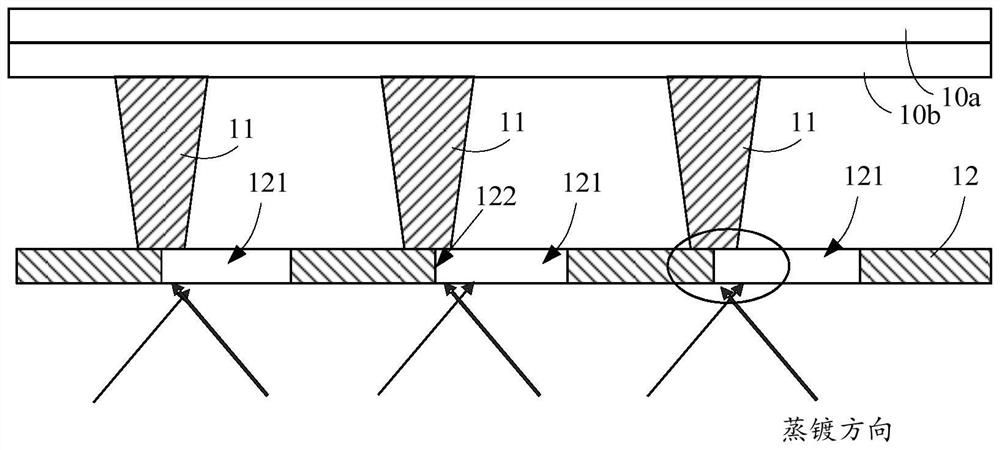
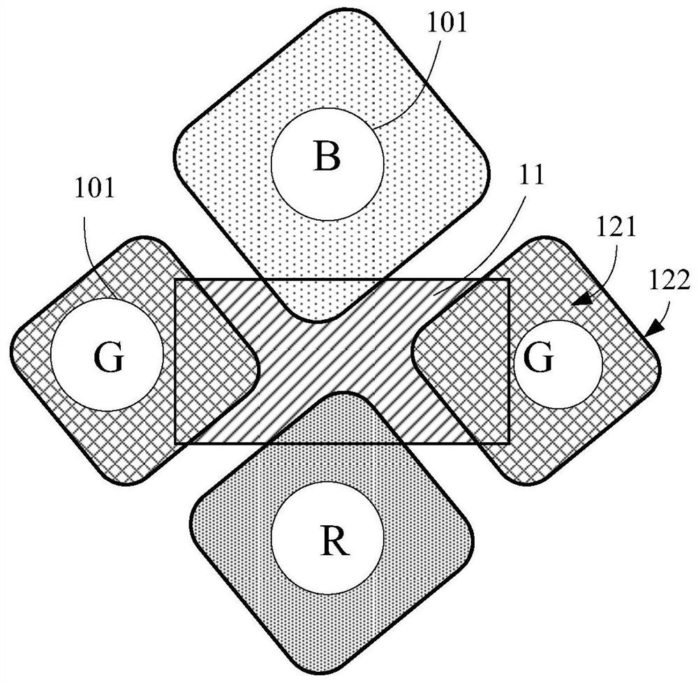
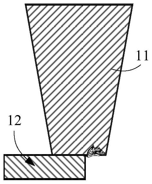
[0030] The following will clearly and completely describe the technical solutions in the embodiments of the present application with reference to the accompanying drawings in the embodiments of the present application. Obviously, the described embodiments are only part of the embodiments of the present application, not all of them. Based on the embodiments in this application, all other embodiments obtained by persons of ordinary skill in the art without making creative efforts belong to the scope of protection of this application.

[0031] The terms "first", "second", and "third" in this application are used for descriptive purposes only, and cannot be understood as indicating or implying relative importance or implicitly specifying the quantity of indicated technical features. Thus, features defined as "first", "second", and "third" may explicitly or implicitly include at least one of these features. In the description of the present application, "plurality" means at least t...


PUM


Abstract

The invention provides a display panel, a preparation method thereof and a display device. The display panel comprises a substrate, a pixel limiting layer and a plurality of supporting columns, wherein the pixel defining layer is formed on the substrate and is defined to form a plurality of pixel areas; the supporting columns are arranged on the surface of the side, away from the substrate, of the pixel limiting layer and located between the adjacent pixel areas; wherein an avoiding part is formed on the supporting column, so that the opening edge of the mask plate is suspended through the avoiding part. The display panel can effectively guarantee the flatness of the surface of the side, deviating from the substrate, of the supporting column, improves the reliability of product packaging, and reduces the occurrence probability of abnormal product display.

Description

technical field [0001] The invention relates to the field of display technology, in particular to a display panel, a manufacturing method thereof, and a display device. Background technique [0002] Organic light emission diode (OLED) display devices are widely favored in the display technology industry due to their luminous effect and the advantages of thinness, flexibility, and high color contrast in display. [0003] Currently, see figure 1 , figure 1 It is a schematic diagram of the structure of vapor-depositing organic materials through fine metal masks in the prior art; in the preparation process of OLED organic light-emitting layer, organic materials need to be vapor-deposited on the substrate prepared with thin-film transistors through fine metal masks , to form R / G / B organic light-emitting layers respectively. Among them, in the evaporation chamber, in order to prevent the fine metal mask from directly contacting the substrate and scratching the substrate film la...

Claims


Application Information

Patent Timeline
Patent Type & Authority Applications(China)
IPC IPC(8): H01L27/32H01L51/52H01L51/56
CPCH10K59/122H10K50/8428H10K71/00
Inventor 孙琳李世泰李慧
Owner HEFEI VISIONOX TECH CO LTD
Why Eureka
Try Eureka