Defectivity and process control of electroless deposition in microelectronics applications

a technology of electroless deposition and process control, applied in the direction of liquid/solution decomposition chemical coating, semiconductor/solid-state device details, non-metal conductors, etc., can solve the problems of electrical short, disrupt electrical flow, and damage to the device, so as to reduce the spontaneous decomposition of the bath, suppress nodular growth, and extensive hydrogen evolution

Active Publication Date: 2007-03-22
MACDERMID ENTHONE INC
View PDF75 Cites 10 Cited by
  • Summary
  • Abstract
  • Description
  • Claims
  • Application Information

AI Technical Summary

Benefits of technology

[0018] Stabilizers: additives for an electroless plating composition that reduce spontaneous decomposition of the bath and uncontrollable precipitation of the metal in the volume of the solution. For example, stabilizers suppress nodular, stray growth, and extensive hydrogen evolution, thereby preventing pitting.
[0019] Levelers: additives for an electroless plating composition that help to equalize the growth rate of the Co film on different Cu grains and at Cu grain interfaces, on different size features, features located in different areas, dense and isolated, and / or features with different surface areas. Thus, levelers promote formation of an electroless Co film with even morphology, low roughness, and uniform thickness of Co on different Cu features.
[0020] Grain refiners: additives for an electroless plating composition that promote formation of the electroless film with uniformly sized grains and smooth grain interfaces. Grain refiners, consequently, reduce granularity of the deposit and improve roughness.

Problems solved by technology

Such diffusion can be detrimental to the device because it can cause electrical leakage in substrates, or form an unintended electrical connection between two interconnects resulting in an electrical short.
Moreover, Cu diffusion out of an interconnect feature can disrupt electrical flow.
Copper also has a tendency to migrate from one location to another when electrical current passes through interconnect features in service, creating voids and hillocks.
This migration can damage an adjacent interconnect line and disrupt electrical flow in the feature where the metal migrates.
Accordingly, among the challenges facing integrated circuit device manufacturers is to minimize diffusion and electromigration of metal in metal-filled interconnect features.
This challenge becomes more acute as the devices further miniaturize, and as the features further miniaturize and densify.
Another challenge in the context of metal interconnect features is to protect them from corrosion.
Certain interconnect metals, especially Cu, are more susceptible to corrosion.
This reactivity can undermine adhesion to dielectrics and thin films, resulting in voids and delamination.
Another challenge is therefore to combat oxidation and enhance adhesion between the cap and the Cu, and between structure layers.
A particular problem for the integration of this technology to current ULSI fabrication lines is high defectivity of the capping layer.
Defectivity reduction remains a challenge in ULSI fabrication lines.
This problem may be generally caused by a lack of stability of the working bath, and formation of incubation centers in the solution, such as Co3+ due to the oxidation of Co2+ by dissolved oxygen.
Those defects decrease diffusion barrier effectiveness, lower the capability of the capping layer to suppress electromigration, cause electromigration failure, affect the signal propagation across the circuitry, increase current leakage, and may even result in electrical shorts.

Method used


Image

  • Defectivity and process control of electroless deposition in microelectronics applications
  • Defectivity and process control of electroless deposition in microelectronics applications
  • Defectivity and process control of electroless deposition in microelectronics applications

Examples


example 1

Electroless Deposition Composition Comprising Stabilizer for Plating Ternary Alloy Comprising Co—W—P

[0078] A first electroless plating bath was prepared comprising the following components:

[0079] 20-40 g / L CoCl2.6H2O

[0080] 40-80 g / L C6H8O7 (citric acid)

[0081] 10-30 g / L H3BO3 (boric acid)

[0082] 4-12 g / L H2WO4 (tungstic acid)

[0083] 10-20 g / L H3PO2 (hypophosphorous acid)

[0084] 10-30 ppm CH3C(═NOH) C(═NOH)CH3 (dimethylglyoxime)

[0085] The electroless plating bath (1 L) was prepared at room temperature by preparing two solutions separately, Solution A (500 mL) and Solution B (500 mL), and combining the solutions to yield the electroless plating bath.

[0086] To prepare Solution A (500 mL): [0087] 1. CoCl2.6H2O dissolved in water in an amount sufficient, upon dilution to 500 mL, to yield a concentration which was twice the final concentration. [0088] 2. Added citric acid and boric acid to the Co2+ solution. [0089] 3. pH adjusted to about 7.0 using TMAH. [0090] 4. Pre-dissolved tungs...

example 2

Electroless Deposition Composition Comprising Stabilizer for Plating Ternary Alloy Comprising Co—W—P

[0107] A second electroless plating bath was prepared comprising the following components:

[0108] 20-40 g / L CoCl2.6H2O

[0109] 40-80 g / L C6H8O7 (citric acid)

[0110] 10-30 g / L H3BO3 (boric acid)

[0111] 4-12 g / L H2WO4 (tungstic acid)

[0112] 10-20 g / L H3PO2 (hypophosphorous acid)

[0113] 5-30 ppm C7H7NO2 (2-aminobenzoic acid)

[0114] pH adjusted to between 8.0 and 9.5.

[0115] One liter of this bath was prepared at room temperature according to a protocol similar to that described in Example 1.

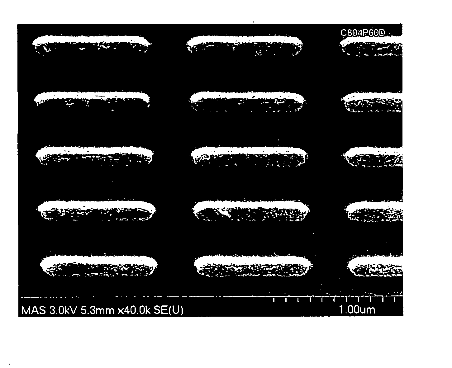
[0116] This bath was used to plate a smooth and uniform deposit of the Co—W—P ternary alloy at a plating bath temperature between 65° C. and 80° C. Plating was initiated by Pd seeding. Plating for about 1 minute yielded a deposit having a thickness between about 100 Å and about 150 Å. Thus, the plating rate was between about 100 Å / min and about 150 Å / min. The deposited Co—W—P ternary alloy had an RMS...

example 3

Electroless Deposition Composition Comprising Stabilizer for Plating Quaternary Alloy Comprising Co—W—Mo—P

[0117] A third electroless plating bath was prepared comprising the following components:

[0118] 20-40 g / L CoCl2.6H2O

[0119] 40-80 g / L C6H8O7 (citric acid)

[0120] 0-30 g / L H3BO3 (boric acid)

[0121] 2-6 g / L H2WO4 (tungstic acid)

[0122] 5-15 g / L H3PO2 (hypophosphorous acid)

[0123] 200-300 ppm Calfax 10LA-75 (Pilot Chemical Co.)

[0124] 50-250 ppm MoO3 (Molybdenum oxide)

[0125] pH adjusted to between 8.0 and 9.5.

[0126] One liter of this bath was prepared at room temperature according to a protocol similar to that described in Example 1.

[0127] This bath was used to plate a smooth and uniform deposit of the Co—W—Mo—P quaternary alloy at a plating bath temperature between 65° C. and 80° C. Plating was initiated by Pd seeding. Plating for about 1 minute yielded a deposit having a thickness between about 140 Å and about 180 Å. Thus, the plating rate was between about 140 Å / min and abo...


PUM

PropertyMeasurementUnit
concentrationaaaaaaaaaa

Abstract

Methods and compositions for electrolessly depositing Co, Ni, or alloys thereof onto a substrate in manufacture of microelectronic devices. Grain refiners, levelers, oxygen scavengers, and stabilizers for electroless Co and Ni deposition solutions.

Description

REFERENCE TO RELATED APPLICATION [0001] This is a continuation-in-part application of Ser. No. 11 / 230,912 filed Sep. 20, 2005.FIELD OF THE INVENTION [0002] This invention relates to electroless plating of Co, Ni, and alloys thereof in microelectronic device applications. More specifically, this invention relates to additives including stabilizers, levelers, grain refiners, and oxygen scavengers in Co and Ni electroless plating baths for microelectronic application. BACKGROUND OF THE INVENTION [0003] Electroless deposition of Co is performed in a variety of applications in the manufacture of microelectronic devices. For example, Co is used in capping of damascene Cu metallization employed to form electrical interconnects in integrated circuit substrates. Copper can diffuse rapidly into a Si substrate and dielectric films such as, for example, SiO2 or low k dielectrics. Copper can also diffuse into a device layer built on top of a substrate in multilayer device applications. Such diff...

Claims


Application Information

Patent Timeline
Patent Type & Authority Applications(United States)
IPC IPC(8): H01L21/44
CPCC09D5/10C23C18/34C23C18/50H01L21/288H01L2924/0002H01L21/76849H01L2924/00C23C18/32
Inventor CHEN, QINGYUNVALVERDE, CHARLESPANECCASIO, VINCENTPETROV, NICOLAISTRITCH, DANIELWITT, CHRISTIANHURTUBIES, RICHARD
Owner MACDERMID ENTHONE INC
Why Eureka
Try Eureka