Multi-layer PCB laminated structure system and method

A stacked structure, PCB board technology, applied in the direction of multi-layer circuit manufacturing, structural connection of printed circuit, electrical components, etc., can solve the problem of inconvenient connection of multi-layer PCB, so as to save resources, prevent contact and avoid being scratch effect

Pending Publication Date: 2022-03-22
深圳市源诚泰电子有限公司
View PDF0 Cites 0 Cited by
  • Summary
  • Abstract
  • Description
  • Claims
  • Application Information

AI Technical Summary

Problems solved by technology

[0003] In order to solve the problems raised in the above-mentioned background technology, the object of the present invention is to provide a multi-layer PCB stacking structure system and method, which has the advantage of being convenient for staff to connect, and solves the problem that multi-layer PCB is inconvenient for staff to connect

Method used


Image

  • Multi-layer PCB laminated structure system and method
  • Multi-layer PCB laminated structure system and method
  • Multi-layer PCB laminated structure system and method

Examples


Embodiment Construction

[0030] The following will clearly and completely describe the technical solutions in the embodiments of the present invention with reference to the accompanying drawings in the embodiments of the present invention. Obviously, the described embodiments are only some, not all, embodiments of the present invention. Based on the embodiments of the present invention, all other embodiments obtained by persons of ordinary skill in the art without making creative efforts belong to the protection scope of the present invention.

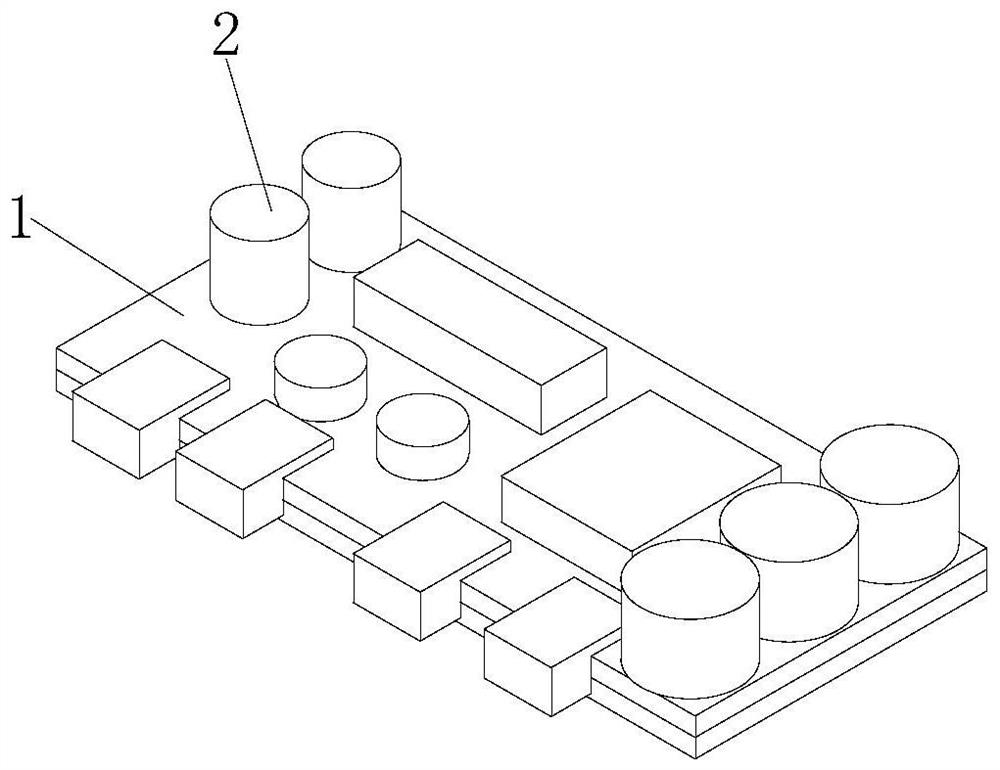
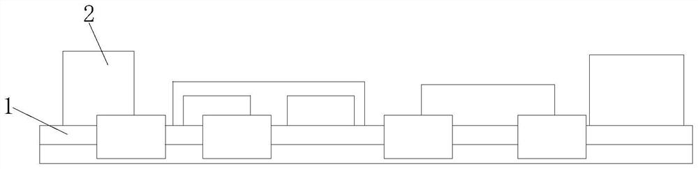
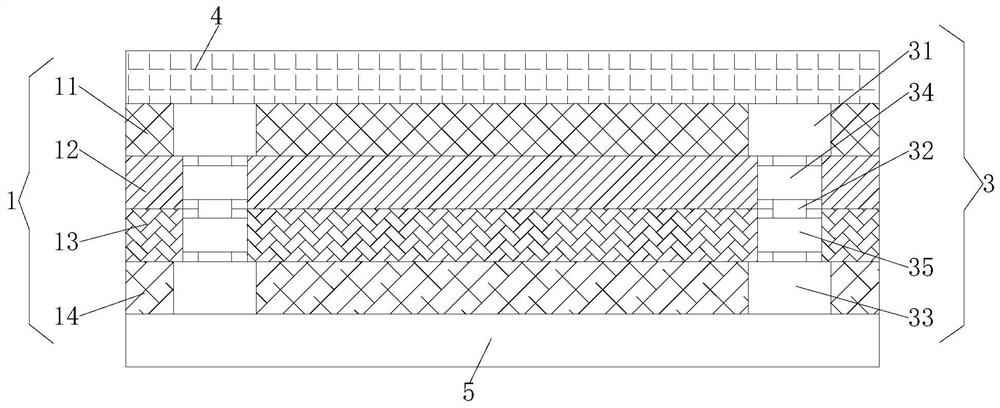
[0031] Such as Figure 1 to Figure 6 As shown, a kind of multilayer PCB lamination structure system provided by the present invention comprises multilayer PCB board 1, and the top of multilayer PCB board 1 is fixedly connected with PCB board element 2, and multilayer PCB board 1 comprises PCB board one 11, PCB The bottom of board one 11 is movably connected with PCB board two 12, the bottom of PCB board two 12 is fixedly connected with PCB board three 13, the ...


PUM


Abstract

The invention discloses a multi-layer PCB laminated structure system, which comprises a multi-layer PCB, the top of the multi-layer PCB is fixedly connected with a PCB element, the multi-layer PCB comprises a first PCB, the bottom of the first PCB is movably connected with a second PCB, the bottom of the second PCB is fixedly connected with a third PCB, the bottom of the third PCB is fixedly connected with a fourth PCB, and the PCB element is fixedly connected with the PCB element. Connecting mechanisms are arranged on the two sides of the top of the first PCB. According to the multi-layer PCB stacking structure system and method, by arranging the connecting mechanisms, the phenomenon that the first PCB, the second PCB, the third PCB and the fourth PCB in the multi-layer PCBs deviate can be prevented, the effect of facilitating connection of workers is achieved, the problem that the multi-layer PCBs are inconvenient to connect by the workers is solved, the multi-layer PCB stacking structure system and method have the advantage of facilitating connection of the workers, and the working efficiency of the workers is improved. Therefore, the multilayer PCB can be used normally, scrap treatment is avoided, a large amount of resources are saved, and the cost of the multilayer PCB is reduced.

Description

technical field [0001] The invention relates to the technical field of multilayer PCBs, in particular to a multilayer PCB stacking structure system and method. Background technique [0002] Multi-layer PCB refers to a circuit board that connects multiple PCBs together. When multi-layer PCBs are stacked, it is impossible to avoid the phenomenon that multi-layer PCBs are prone to offset when stacked, which makes it inconvenient for staff to connect, resulting in multi-layer PCBs not being able to work normally. If used, it needs to be scrapped, which wastes a lot of resources and increases the cost of multi-layer PCB. Contents of the invention [0003] In order to solve the problems raised in the above-mentioned background technology, the object of the present invention is to provide a multi-layer PCB stacking structure system and method, which has the advantage of being convenient for workers to connect, and solves the problem that multi-layer PCBs are inconvenient for work...

Claims


Application Information

Patent Timeline
IPC IPC(8): H05K1/14H05K1/02H05K3/46
CPCH05K1/144H05K1/02H05K1/0209H05K1/0298H05K3/4611
Inventor 蔡明成蔡明芳
Owner 深圳市源诚泰电子有限公司
Why Eureka
Try Eureka