Wireless charging LED lamp based on environment radio frequency signal
A technology of LED lights and radio frequency signals, applied in current collectors, electric vehicles, electrical components, etc., can solve problems such as energy waste, improve absorption efficiency, avoid energy waste and space occupation, and reduce reflection loss.
- Summary
- Abstract
- Description
- Claims
- Application Information
AI Technical Summary
Problems solved by technology
Method used
Image


Examples
Embodiment Construction
[0029] The following will clearly and completely describe the technical solutions in the embodiments of the present invention with reference to the accompanying drawings in the embodiments of the present invention. Obviously, the described embodiments are only some, not all, embodiments of the present invention. Based on the embodiments of the present invention, all other embodiments obtained by persons of ordinary skill in the art without making creative efforts belong to the protection scope of the present invention.
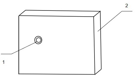
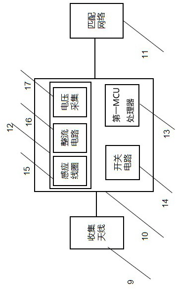
[0030] like figure 1 As shown, the present invention provides a wireless charging LED lamp based on environmental radio frequency signals, including an LED lamp 1 and a lamp body 2 for installing the LED lamp 1 , and the LED lamp 1 is installed on the front of the lamp body 2 . like figure 2 As shown, the lamp body 2 is provided with a control module 3, a power supply module 4 and an energy storage module 5. The control module is used to control the working ...
PUM
 Abstract
Description
Claims
Application Information
PatSnap Eureka turns technology decisions into work you can execute. Powered by our Innovation Knowledge Graph, it runs expert workflows across engineering, life sciences, materials and intellectual property. Get your review-ready output in minutes.


