
Wafer die exposure field arrangement method, wafer preparation method and wafer

An exposure field and die technology, applied in the field of chip manufacturing, can solve the problems of low effective utilization of wafers, increase the number of scrapped dies, and a small number of die arrangements, and reduce the number of scrapped dies, increase the number, Take advantage of the effect

Pending Publication Date: 2022-04-05
北海惠科半导体科技有限公司
View PDF0 Cites 0 Cited by
  • Summary
  • Abstract
  • Description
  • Claims
  • Application Information

AI Technical Summary

Problems solved by technology

[0003] However, currently, due to the small overlapping area of ​​the exposure field between the wafer and the die, the overlapping area at the edge of the wafer is not covered, resulting in a small number of die arrangements in the wafer, which in turn leads to a low effective utilization of the wafer
If the arrangement relationship between the die exposure field and the wafer is changed arbitrarily, and the overlapping area at the edge of the wafer is covered as much as possible, it will inevitably cause damage to the dies covered with the wafer when the wafer is subsequently cut. scratches, greatly increasing the number of scrapped die

Method used


Image

  • Wafer die exposure field arrangement method, wafer preparation method and wafer
  • Wafer die exposure field arrangement method, wafer preparation method and wafer
  • Wafer die exposure field arrangement method, wafer preparation method and wafer

Examples


Embodiment Construction

[0040] In order to make the purposes, technical solutions and advantages of the embodiments of the present application clearer, the technical solutions in the embodiments of the present application will be clearly and completely described below in conjunction with the drawings in the embodiments of the present application. Obviously, the described embodiments It is a part of the embodiments of this application, but not all of them. Based on the embodiments in the present application, all other embodiments obtained by persons of ordinary skill in the art without making creative efforts belong to the protection scope of the present application.

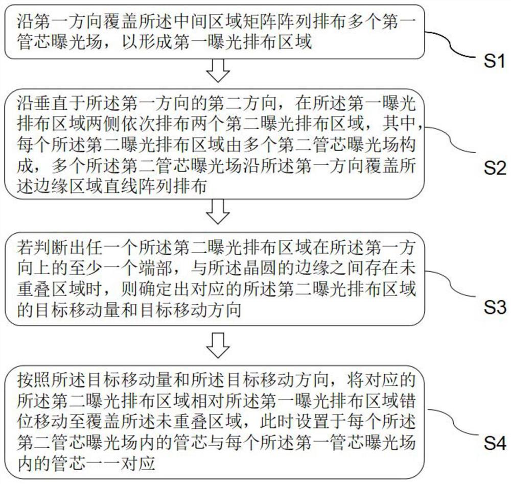
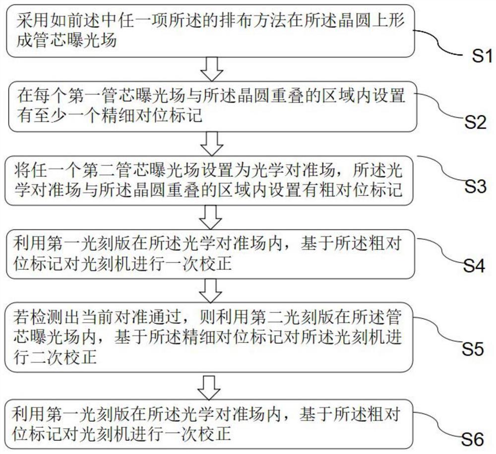
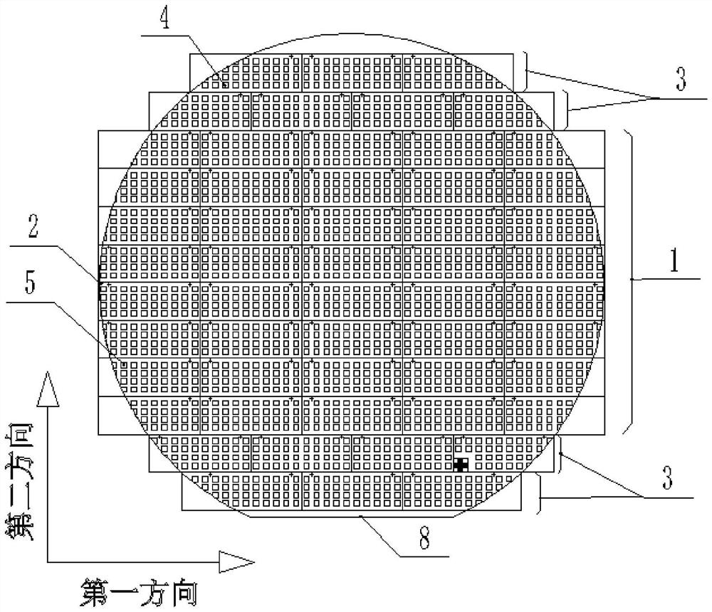
[0041] like figure 1 and Figure 4 As shown, the embodiment of the present application provides a method for arranging the exposure field of wafer dies. The wafer is divided into a middle area and edge areas arranged on both sides of the middle area. More specifically, the wafer A flat edge 8 is provided on the top, for the convenienc...


PUM


Abstract

The invention relates to a wafer tube core exposure field arrangement method, a wafer preparation method and a wafer, and the method specifically comprises the following steps: firstly forming a first exposure arrangement region and second exposure arrangement regions, and then determining at least one end part of any second exposure arrangement region in a first direction; when a non-overlapping area exists between the die exposure field and the edge of the wafer, the target movement amount and the target movement direction of the corresponding second exposure arrangement area are determined, and the non-overlapping area formed at the edge of the wafer is covered by adopting the dislocation movement mode, so that the overlapping area of the die exposure field and the wafer is increased, and the yield of the die exposure field is improved. The number of the tube cores on a single wafer is increased, the effective area of the wafer is fully utilized, and the yield of the tube cores on the single wafer is increased; in addition, the die array in the first die exposure field and the die array in the moved second die exposure field are aligned, so that the die is prevented from being scratched when the wafer is cut.

Description

technical field [0001] The present application relates to the technical field of chip manufacturing, and in particular to a method for arranging exposure fields of wafer dies, a method for preparing a wafer, and the wafer. Background technique [0002] At present, the die lithography process uses a UT lithography machine to perform step-by-step exposure on the wafer, and then lithographically etches fine structures onto the wafer. A stepping unit is a die exposure field, and a plurality of dies are arranged in a matrix in each die exposure field. Through each step, the exposure field of a single die is arranged to fill the entire wafer, thereby realizing that the entire wafer is covered with dies. [0003] However, currently, due to the small overlapping area of ​​the exposure field between the wafer and the die, the overlapping area at the edge of the wafer is not covered, resulting in a small number of dies in the wafer, which in turn leads to a low effective utilization ...

Claims


Application Information

Patent Timeline
Patent Type & Authority Applications(China)
IPC IPC(8): G03F7/20
Inventor 王占伟王国峰
Owner 北海惠科半导体科技有限公司
Features
  • Generate Ideas
  • Intellectual Property
  • Life Sciences
  • Materials
  • Tech Scout
  • Unparalleled Data Quality
  • Higher Quality Content
  • 60% Fewer Hallucinations
Learn More