Electro-optical silicon-based modulator traveling wave electrode with suspended metal shielding wire

A metal shielding, traveling wave electrode technology, applied in nonlinear optics, instruments, optics, etc., can solve the problems of low degree of freedom, difficult design indicators, low microwave loss, etc., to achieve low microwave loss, reduce electric field distribution, and save development. cost effect

Pending Publication Date: 2022-04-12
HUAZHONG UNIV OF SCI & TECH
View PDF7 Cites 0 Cited by
  • Summary
  • Abstract
  • Description
  • Claims
  • Application Information

AI Technical Summary

Problems solved by technology

[0005] Aiming at the defects of related technologies, the purpose of the present invention is to provide a traveling-wave electrode for an electro-optic silicon-based modulator with suspended metal shielding wires, aiming to solve the problem of low design freedom of traditional traveling-wave electrodes in electro-optic silicon-based modulators. It is necessary to meet the difficult problems of design indicators such as impedance matching, speed matching, and lower microwave loss at the same time, so that impedance matching, speed matching, and microwave loss reduction can be realized at a lower cost without the need for customized process steps

Method used


Image

  • Electro-optical silicon-based modulator traveling wave electrode with suspended metal shielding wire
  • Electro-optical silicon-based modulator traveling wave electrode with suspended metal shielding wire
  • Electro-optical silicon-based modulator traveling wave electrode with suspended metal shielding wire

Examples


Embodiment 1

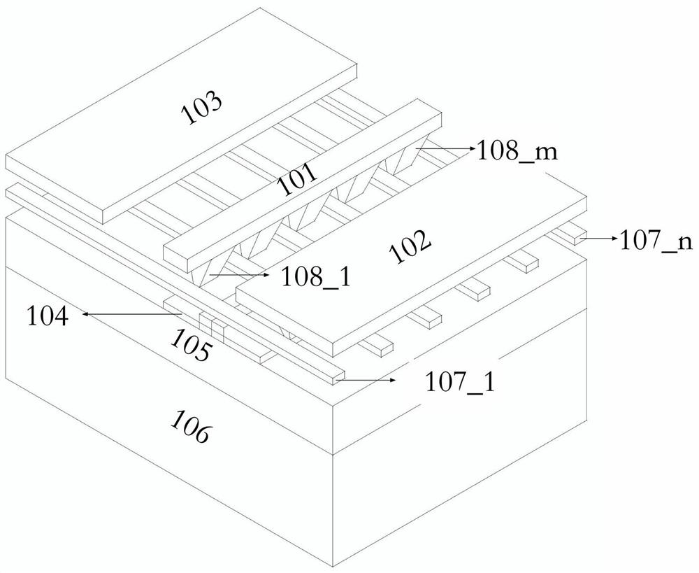
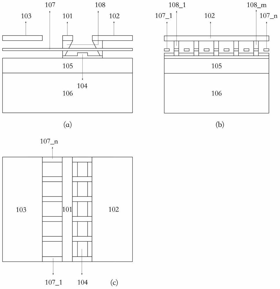
[0044] The schematic diagram of the electro-optic silicon-based modulator coplanar waveguide type traveling wave electrode with suspended metal shielding wires proposed in the embodiment of the present invention is shown in the description of the drawings figure 1 with figure 2shown. It consists of a signal line 101, a first ground plane 102, a second ground plane 103, an optical waveguide 104, a buried oxide layer 105, a substrate layer 106, and a suspended metal shielding line 107 (including 107_1 to 107_n, wherein n is an integer greater than 1) and stacked vias 108 (including 108_1 to 108_m, wherein m is an integer greater than 1). The optical waveguide is located above the buried oxide layer and is composed of P-type doped and N-type doped silicon materials, and is connected to the upper signal line and the first ground plane through stacked via holes. The second ground plane is not connected to the optical waveguide. The signal line is located at the same level as th...

Embodiment 2

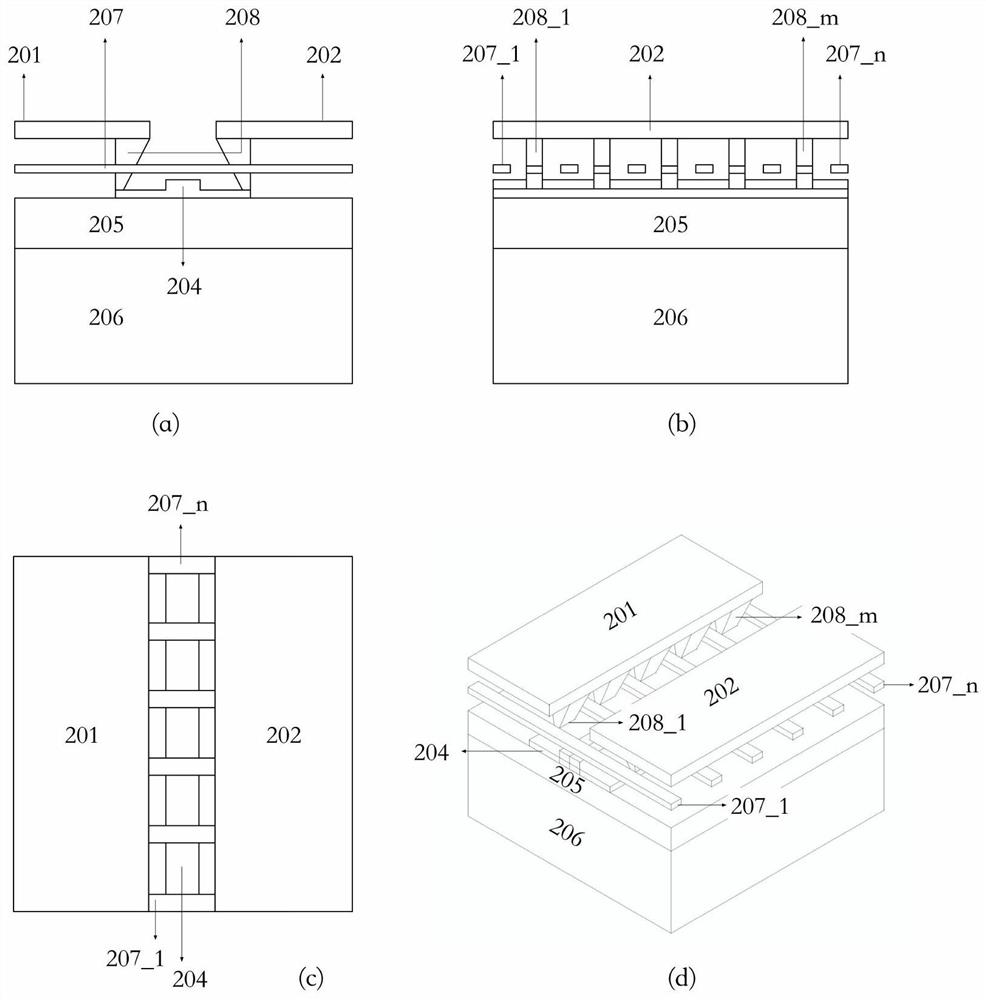
[0047] The schematic diagram of the electro-optic silicon-based modulator coplanar slot-line type traveling wave electrode with suspended metal shielding lines proposed in the embodiment of the present invention is shown in the description of the drawings image 3 shown. It consists of a signal line 201, a first ground plane 202, an optical waveguide 204, a buried oxide layer 205, a substrate layer 206, a suspended metal shielding line 207 (including 207_1 to 207_n, wherein n is an integer greater than 1) and stacked vias 208 ( Including 208_1 to 208_m, wherein m is an integer greater than 1). The optical waveguide is located above the buried oxide layer and is composed of P-type doped and N-type doped silicon materials, and is connected to the upper signal line and the first ground plane through stacked via holes. The signal line is located on the same level as the first ground plane. The suspended metal shielding line is located between the optical waveguide and the horizo...

Embodiment 3

[0050] The schematic diagram of the electro-optic silicon-based modulator coplanar waveguide traveling-wave electrode with suspended metal shielding wires and track electrodes proposed in the embodiment of the present invention is shown in the description of the drawings Figure 4 shown. It consists of a signal line 301, a first ground plane 302, a second ground plane 303, an optical waveguide 304, a buried oxide layer 305, a substrate layer 306, and a suspended metal shielding line 307 (including 307_1 to 307_n, wherein n is an integer greater than 1) , stacked vias 308 (including 308_1 to 308_m, wherein m is an integer greater than 1) and track electrodes 309_1 to 309_k (k is an integer greater than 1). The optical waveguide is located above the buried oxide layer and is composed of P-type doped and N-type doped silicon materials, and is connected to the upper signal line and the first ground plane through stacked via holes. The second ground plane is not connected to the o...


PUM


Abstract

The invention discloses an electro-optical silicon-based modulator traveling wave electrode with a suspended metal shielding wire, and belongs to the field of electro-optical modulators. Comprising a signal line, a first ground plane, an optical waveguide, a suspended metal shielding line and stacked through holes, the signal line and the first ground plane are positioned on the same horizontal plane above the optical waveguide; the optical waveguide is connected with the signal line and the first ground plane at the same time through a plurality of stacked through holes; and the suspended metal shielding wires pass through gaps among the plurality of stacked through holes and are arranged periodically. The design requirements of impedance matching, speed matching and low microwave loss can be met at the same time, additional design freedom is introduced to the traveling wave electrode on the premise that process steps do not need to be customized, parameters of the traveling wave electrode can be flexibly optimized, and the development cost is effectively saved.

Description

technical field [0001] The invention belongs to the field of electro-optic modulators, and more specifically relates to a traveling-wave electrode of an electro-optic silicon-based modulator with suspended metal shielding wires. Background technique [0002] In the design of electro-optic silicon-based modulators, traveling-wave electrodes are a common technical solution for driving optical waveguides. In order to improve the electro-optic bandwidth of electro-optic silicon-based modulators, the design of traveling-wave electrodes usually takes three factors into consideration. The first is to make the characteristic impedance of the traveling wave electrode better match the terminal impedance of the input and output; the second is to realize the transmission speed of the microwave signal on the traveling wave electrode and the group velocity of the optical signal in the optical waveguide. Better matching; the third is to reduce the microwave loss of the traveling wave elec...

Claims


Application Information

Patent Timeline
Patent Type & Authority Applications(China)
IPC IPC(8): G02F1/025
Inventor 谭旻叶开轩
Owner HUAZHONG UNIV OF SCI & TECH
Why Eureka
Try Eureka