AOI automatic optical detector for appearance detection of circuit board line

An automatic optical inspection, circuit board circuit technology, applied in optical testing flaws/defects, scientific instruments, material analysis by optical means, etc. Reduce the effect of manual intervention

Inactive Publication Date: 2022-04-15
深圳易科讯科技有限公司
View PDF0 Cites 2 Cited by
  • Summary
  • Abstract
  • Description
  • Claims
  • Application Information

AI Technical Summary

Problems solved by technology

[0003] The AOI automatic optical inspection instrument mainly consists of a detection camera and a PCB transmission component. When in use, it mainly relies on manually putting the PCB into the PCB transmission component and limiting the PCB, and then opens the transmission component to push the PCB into the interior of the automatic optical inspection instrument. At this time, the instrument will start the camera and drive the camera to move to take pictures of the PCB part. After the pictures are taken, use its own software to analyze and reflect to the operator through the display. Although the detector can liberate the traditional manual inspection, it is only in the inspection part. Fully automatic is realized. During the entire PCB inspection process, the operator still needs to place the PCB boards on the transmission assembly one by one, and after the limit, start the transmission assembly. After the inspection is completed, it needs to be taken out manually, and the degree of automation is low. , in the large-scale PCB inspection process, it still takes a lot of time for the loading stage, and it is impossible to realize the PCB loading one by one to increase the automation of the detector
[0004] With the increasing integration of PCB circuit boards, more and more electronic components are installed on a single PCB, resulting in too dense components on the surface of the PCB, so the traditional single-sided PCB can no longer meet the requirements of today's precision equipment. demand, so there is a double-sided PCB board with higher integration. When the appearance inspection of the double-sided PCB board is required, it is necessary to put the front side of the PCB board into the transmission component of the AOI optical detector, and use the optical detector After testing the front side of the PCB board, after the PCB board is exported, the PCB board is manually turned over and then pushed into the inside of the optical detector for reverse side detection, resulting in a decrease in the detection efficiency of the double-layer PCB board and affecting the PCB board. quality
[0005] Since the production and testing of PCB boards are not carried out in a clean room, the surface of the PCB board will be contaminated with a certain amount of dust. Although these fine dusts will not affect the performance of the PCB, but the PCB board with fine dust When entering the interior of the AOI optical detector, because the camera inside the AOI optical detector will enlarge the PCB, the fine dust will be enlarged accordingly. At this time, the enlarged fine dust will often be regarded as a defect by the machine, and then NG phenomenon will appear. It is necessary to manually remove the PCB and clean it before continuing the inspection, which affects the inspection time

Method used


Image

  • AOI automatic optical detector for appearance detection of circuit board line
  • AOI automatic optical detector for appearance detection of circuit board line
  • AOI automatic optical detector for appearance detection of circuit board line

Examples


Embodiment Construction

[0032] The following will clearly and completely describe the technical solutions in the embodiments of the present invention with reference to the accompanying drawings in the embodiments of the present invention. Obviously, the described embodiments are only some, not all, embodiments of the present invention. Based on the embodiments of the present invention, all other embodiments obtained by persons of ordinary skill in the art without making creative efforts belong to the protection scope of the present invention.

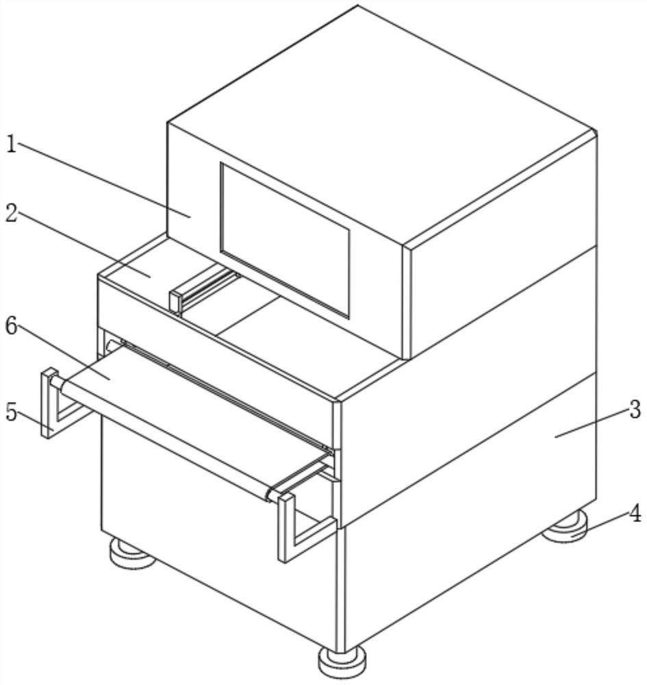
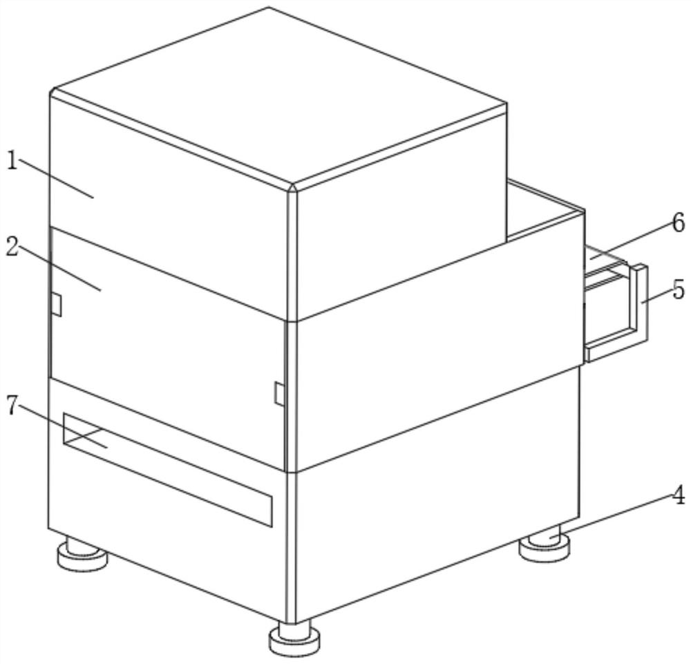
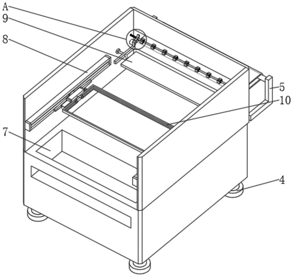
[0033] like figure 1 and figure 2 as well as image 3 and Figure 4 As shown, in the embodiment of the present invention, an AOI automatic optical detector for the appearance detection of a circuit board circuit includes an AOI detector body 1, and a detection box 2 is fixedly installed at the bottom of the AOI detector body 1, and the detection box 2 The base 3 is fixedly installed at the bottom, and the left and right sides of the front of the detection ...


PUM


Abstract

The invention belongs to the technical field of PCB detection, and discloses an AOI automatic optical detector for appearance detection of a circuit board line, the AOI automatic optical detector comprises an AOI detector body, the bottom end of the AOI detector body is fixedly provided with a detection box, the bottom end of the detection box is fixedly provided with a base, and the left and right sides of the front surface of the detection box are fixedly provided with support frames. A first servo motor is started to drive a main shaft to rotate so as to drive a movable rod to rotate, at the moment, the movable rod can apply pressure to a lever, the lever is driven by a U-shaped rod to deflect towards the inner side and drive a discharging plate to deflect towards the inner side, and a PCB slides towards the inner side along with the lever, falls into the upper portion of a containing frame and falls into a clamping groove; at the moment, the electric guide rail is reversely started to drive the sliding block and the placing frame to move towards the inner side, the movable rod does not make contact with the lever any more, the power source of the conveying belt is turned off, conveying is stopped, automatic discharging of the single PCB is completed, the manual intervention degree is reduced, and therefore the advantage of automatic discharging is achieved.

Description

technical field [0001] The invention belongs to the technical field of PCB detection, in particular to an AOI automatic optical detector for appearance detection of circuit board circuits. Background technique [0002] The full name of AOI in Chinese is Automatic Optical Inspection, which is a device based on optical principles to detect common defects encountered in welding production. AOI is a new type of testing technology that has emerged, but it has developed rapidly. Many manufacturers have introduced AOI testing. Equipment, when automatic detection, the machine automatically scans the PCB through the camera, collects images, compares the tested solder joints with the qualified parameters in the database, and after image processing, checks out the defects on the PCB, and displays the defects through the display or automatic signs / Marked out for repairing by maintenance personnel. It mainly uses high-speed and high-precision visual processing technology to automaticall...

Claims


Application Information

Patent Timeline
Patent Type & Authority Applications(China)
IPC IPC(8): G01N21/89G01N21/13G01N21/01
Inventor 李祥易中群
Owner 深圳易科讯科技有限公司
Why Eureka
Try Eureka